ADP3212/NCP3218
and low-side FETs are off and no current flows into the inductor
(see Figure 17). Figure 18 shows the inductor current and switch
node voltage in DCM.
OFF
OFF
L
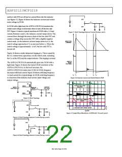
In DCM with a light load, the ADP3212/NCP3218 monitors the
switch node voltage to determine when to turn off the low-side
FET. Figure 19 shows a typical waveform in DCM with a 1 A load
current. Between t1 and t2, the inductor current ramps down. The
current flows through the source drain of the low-side FET and
creates a voltage drop across the FET with a slightly negative
switch node. As the inductor current ramps down to 0 A, the
switch voltage approaches 0 V, as seen just before t2. When the
switch voltage is approximately −6 mV, the low-side FET is
turned off.
C
LOAD
Figure 17. Buck Topology Inductor Current During t2 and t3
INDUCTOR
CURRENT
Figure 18 shows a small, dampened ringing at t2. This is caused by
the LC created from capacitance on the switch node, including
the CDS of the FETs and the output inductor. This ringing is normal.
SWITCH
NODE
VOLTAGE
The ADP3212/NCP3218 automatically goes into DCM with a
light load. Figure 19 shows the typical DCM waveform of the
ADP3212/NCP3218. As the load increases, the
ADP3212/NCP3218 enters into CCM. In DCM, frequency
decreases with load current. Figure 20 shows switching frequency
vs. load current for a typical design. In DCM, switching frequency
is a function of the inductor, load current, input voltage, and
output voltage.
t0 t1
t2
t3 t4
Figure 18. Inductor Current and Switch Node in DCM
4
Q1
OUTPUT VOLTAGE
20mV/DIV
DRVH
OUTPUT
VOLTAGE
INPUT
VOLTAGE
SWITCH
NODE
L
Q2
SWITCH NODE 5V/DIV
C
LOAD
DRVL
2
Figure 14. Buck Topology
INDUCTOR CURRENT
5A/DIV
3
1
ON
L
LOW-SIDE GATE DRIVE 5V/DIV
2µs/DIV
C
LOAD
OFF
Figure 19. Single-Phase Waveforms in DCM with 1 A Load Current
Figure 15. Buck Topology Inductor Current During t0 and t1
OFF
L
C
LOAD
ON
Figure 16. Buck Topology Inductor Current During t1 and t2
Rev. SpA | Page 22 of 43

 ONSEMI [ ONSEMI ]