ADP3212/NCP3218
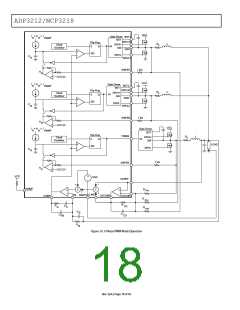
VDC
positioning setpoint. The arrangement results in an enhanced
feedforward response.
Phase 1
Inductor
ADP3212
SWFB1
RSWFB1
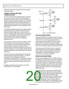
CURRENT CONTROL MODE AND
THERMAL BALANCE
33
28
24
VDC
The ADP3212/NCP3218 has individual inputs for monitoring
the current of each phase. The phase current information is
combined with an internal ramp to create a current-balancing
feedback system that is optimized for initial current accuracy and
dynamic thermal balance. The current balance information is
independent from the total inductor current information used for
voltage positioning described in the Active Impedance Control
Mode section.
Phase 2
Inductor
RSWFB2
SWFB2
SWFB3
VDC
Phase 3
Inductor
RSWFB3
The magnitude of the internal ramp can be set so that the transient
response of the system is optimal. The ADP3212/NCP3218
monitors the supply voltage to achieve feedforward control
whenever the supply voltage changes. A resistor connected from
the power input voltage rail to the RAMP pin determines the
slope of the internal PWM ramp. More detail about
programming the ramp is provided in the Application
Information section.
Figure 11. Current Balance Resistors
VOLTAGE CONTROL MODE
A high-gain bandwidth error amplifier is used for the voltage
mode control loop. The noninverting input voltage is set via the
7-bit VID DAC. The VID codes are listed in Table 6. The
noninverting input voltage is offset by the droop voltage as a
function of current, commonly known as active voltage
positioning. The output of the error amplifier is the COMP pin,
which sets the termination voltage of the internal PWM ramps.
External resistors are placed in series with the SWFB1, SWFB2,
and SWFB3 pins to create an intentional current imbalance.
Such a condition can exist when one phase has better cooling
and supports higher currents the other phases. Resistors
RSWSB1, RSWFB2, and RSWFB3 (see figure 26) can be used to
adjust thermal balance. It is recommended to add these resistors
during the initial design to make sure placeholders are provided
in the layout.
At the negative input, the FB pin is tied to the output sense
location using RB, a resistor for sensing and controlling the
output voltage at the remote sensing point. The main loop
compensation is incorporated in the feedback network
connected between the FB and COMP pins.
To increase the current in any given phase, users should make
RSWFB for that phase larger (that is, RSWFB = 1 k Ω for the
hottest phase and do not change it during balance
optimization). Increasing RSWFB to 1.5 kΩ makes a substantial
increase in phase current. Increase each RSWFB value by small
amounts to achieve thermal balance starting with the coolest
phase.
POWER-GOOD MONITORING
The power-good comparator monitors the output voltage via
the CSREF pin. The PWRGD pin is an open-drain output that
can be pulled up through an external resistor to a voltage rail—
not necessarily the same VCC voltage rail that is running the
controller. A logic high level indicates that the output voltage is
within the voltage limits defined by a range around the VID
voltage setting. PWRGD goes low when the output voltage is
outside of this range.
If adjusting current balance between phases is not needed,
RSWFB should be 1 k Ω for all phases.
Following the IMVP-6.5 specification, the PWRGD range is
defined to be 300 mV less than and 200 mV greater than the
actual VID DAC output voltage. For any DAC voltage less than
300 mV, only the upper limit of the PWRGD range is
monitored. To prevent a false alarm, the power-good circuit is
masked during various system transitions, including a VID
change and entrance into or exit out of deeper sleep. The
duration of the PWRGD mask is set to approximately 130 μs by
an internal timer. If the voltage drop is greater than 200 mV
Rev. SpA | Page 20 of 43

 ONSEMI [ ONSEMI ]