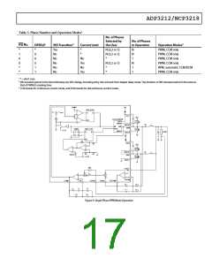
ADP3212/NCP3218
during deeper sleep entry or slow deeper sleep exit, the
duration of PWRGD masking is extended by the internal logic
circuit.
When a VID input changes, the ADP3212/NCP3218 detects the
change but ignores new code for a minimum of 400 ns. This
delay is required to prevent the device from reacting to digital
signal skew while the 7-bit VID input code is in transition.
Additionally, the VID change triggers a PWRGD masking timer
to prevent
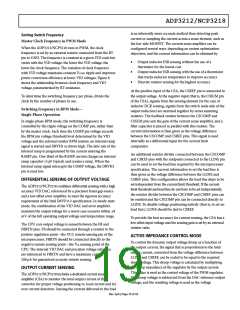
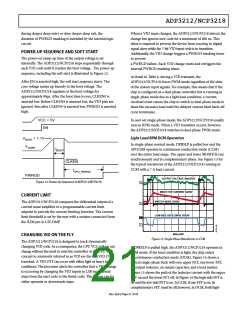
POWER-UP SEQUENCE AND SOFT START
The power-on ramp-up time of the output voltage is set
internally. The ADP3212/NCP3218 steps sequentially through
each VID code until it reaches the boot voltage. The power-up
sequence, including the soft start is illustrated in Figure 12.
a PWRGD failure. Each VID change resets and retriggers the
internal PWRGD masking timer.
As listed in Table 6, during a VID transient, the
After EN is asserted high, the soft start sequence starts. The
core voltage ramps up linearly to the boot voltage. The
ADP3212/NCP3218 regulates at the boot voltage for
approximately 90ꢀs. After the boot time is over, CLKEN# is
asserted low. Before CLKEN# is asserted low, the VID pins are
ignored. 9ms after CLKEN# is asserted low, PWRGD is asserted
high.
ADP3212/NCP3218 forces PWM mode regardless of the state
of the system input signals. For example, this means that if the
chip is configured as a dual-phase controller but is running in
single-phase mode due to a light load condition, a current
overload event causes the chip to switch to dual-phase mode to
share the excessive load until the delayed current limit latch-off
cycle terminates.
In user-set single-phase mode, the ADP3212/NCP3218 usually
runs in RPM mode. When a VID transition occurs, however,
the ADP3212/NCP3218 switches to dual-phase PWM mode.
VCC = 5V
EN
Light Load RPM DCM Operation
V
BOOT = 1.1V
VCORE
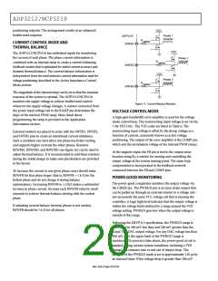
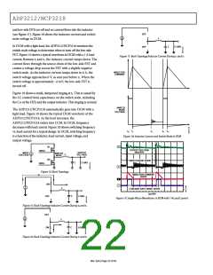
In single-phase normal mode, DPRSLP is pulled low and the
APD3208 operates in continuous conduction mode (CCM)
over the entire load range. The upper and lower MOSFETs run
synchronously and in complementary phase. See Figure 13 for
the typical waveforms of the ADP3212/NCP3218 running in
CCM with a 7 A load current.
tBOOT
CLKEN
tCPU_PWRGD
PWRGD
OUTPUT VOLTAGE 20mV/DIV
4
Figure 12. Power-Up Sequence of ADP3212/NCP3218
INDUCTOR CURRENT 5A/DIV
CURRENT LIMIT
SWITCH NODE 5V/DIV
2
The ADP3212/NCP3218 compares the differential output of a
current sense amplifier to a programmable current limit
setpoint to provide the current-limiting function. The current
limit threshold is set by the user with a resistor connected from
the ILIM pin to CSCOMP.
LOW-SIDE GATE DRIVE 5V/DIV
3
1
400ns/DIV
CHANGING VID ON THE FLY
Figure 13. Single-Phase Waveforms in CCM
The ADP3212/NCP3218 is designed to track dynamically
changing VID code. As a consequence, the CPU VCC voltage can
change without the need to reset the controller or the CPU. This
concept is commonly referred to as VID on-the-fly (VID OTF)
transient. A VID OTF can occur with either light or heavy load
conditions. The processor alerts the controller that a VID change
is occurring by changing the VID inputs in LSB incremental
steps from the start code to the finish code. The change can be
either upwards or downwards steps.
If DPRSLP is pulled high, the ADP3212/NCP3218 operates in
RPM mode. If the load condition is light, the chip enters
discontinuous conduction mode (DCM). Figure 14 shows a
typical single-phase buck with one upper FET, one lower FET,
an output inductor, an output capacitor, and a load resistor.
Figure 15 shows the path of the inductor current with the upper
FET on and the lower FET off. In Figure 16 the high-side FET is
off and the low-side FET is on. In CCM, if one FET is on, its
complementary FET must be off; however, in DCM, both high-
Rev. SpA | Page 21 of 43

 ONSEMI [ ONSEMI ]