ADP3212/NCP3218
is an inherently more accurate method than detecting peak
current or sampling the current across a sense element, such as
the low-side MOSFET. The current sense amplifier can be
configured several ways, depending on system optimization
objectives, and the current information can be obtained by
Setting Switch Frequency
Master Clock Frequency in PWM Mode
When the ADP3212/NCP3218 runs in PWM, the clock
frequency is set by an external resistor connected from the RT
pin to GND. The frequency is constant at a given VID code but
varies with the VID voltage: the lower the VID voltage, the
lower the clock frequency. The variation of clock frequency
with VID voltage maintains constant VCORE ripple and improves
power conversion efficiency at lower VID voltages. Figure 8
shows the relationship between clock frequency and VID
voltage, parameterized by RT resistance.
•
•
•
Output inductor ESR sensing without the use of a
thermistor for the lowest cost
Output inductor ESR sensing with the use of a thermistor
that tracks inductor temperature to improve accuracy
Discrete resistor sensing for the highest accuracy
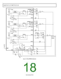
At the positive input of the CSA, the CSREF pin is connected to
the output voltage. At the negative input (that is, the CSSUM pin
of the CSA), signals from the sensing element (in the case of
inductor DCR sensing, signals from the switch node side of the
output inductors) are summed together by series summing
resistors. The feedback resistor between the CSCOMP and
CSSUM pins sets the gain of the current sense amplifier, and a
filter capacitor is placed in parallel with this resistor. The
current information is then given as the voltage difference
between the CSCOMP and CSREF pins. This signal is used
internally as a differential input for the current limit
comparator.
To determine the switching frequency per phase, divide the
clock by the number of phases in use.
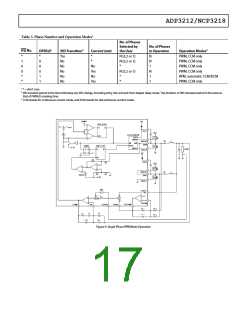
Switching Frequency in RPM Mode—
Single-Phase Operation
In single-phase RPM mode, the switching frequency is
controlled by the ripple voltage on the COMP pin, rather than
by the master clock. Each time the COMP pin voltage exceeds
the RPM pin voltage threshold level determined by the VID
voltage and the external resistor RPM resistor, an internal ramp
signal is started and DRVH1 is driven high. The slew rate of the
internal ramp is programmed by the current entering the
RAMP pin. One-third of the RAMP current charges an internal
ramp capacitor (5 pF typical) and creates a ramp. When the
internal ramp signal intercepts the COMP voltage, the DRVH1
pin is reset low.
An additional resistor divider connected between the CSCOMP
and CSREF pins with the midpoint connected to the LLINE pin
can be used to set the load line required by the microprocessor
specification. The current information to set the load line is
then given as the voltage difference between the LLINE and
CSREF pins. This configuration allows the load line slope to be
set independent from the current limit threshold. If the current
limit threshold and load line do not have to be set independently,
the resistor divider between the CSCOMP and CSREF pins can
be omitted and the CSCOMP pin can be connected directly to
LLINE. To disable voltage positioning entirely (that is, to set no
load line), LLINE should be tied to CSREF.
DIFFERENTIAL SENSING OF OUTPUT VOLTAGE
The ADP3212/NCP3218 combines differential sensing with a high
accuracy VID DAC, referenced by a precision band gap source
and a low offset error amplifier, to meet the rigorous accuracy
requirement of the Intel IMVP-6.5 specification. In steady-state
mode, the combination of the VID DAC and error amplifier
maintain the output voltage for a worst-case scenario within
8
mV of the full operating output voltage and temperature range.
To provide the best accuracy for current sensing, the CSA has a
low offset input voltage and the sensing gain is set by an external
resistor ratio.
The CPU core output voltage is sensed between the FB and
FBRTN pins. FB should be connected through a resistor to the
positive regulation point—the VCC remote sensing pin of the
microprocessor. FBRTN should be connected directly to the
negative remote sensing point—the VSS sensing point of the
CPU. The internal VID DAC and precision voltage reference
are referenced to FBRTN and have a maximum current of
200 μA for guaranteed accurate remote sensing.
ACTIVE IMPEDANCE CONTROL MODE
To control the dynamic output voltage droop as a function of
the output current, the signal that is proportional to the total
output current, converted from the voltage difference between
LLINE and CSREF, can be scaled to be equal to the required
droop voltage. This droop voltage is calculated by multiplying
the droop impedance of the regulator by the output current.
This value is used as the control voltage of the PWM regulator.
The droop voltage is subtracted from the DAC reference output
voltage, and the resulting voltage is used as the voltage
OUTPUT CURRENT SENSING
The ADP3212/NCP3218 includes a dedicated current sense
amplifier (CSA) to monitor the total output current of the
converter for proper voltage positioning vs. load current and for
over current detection. Sensing the current delivered to the load
Rev. SpA | Page 19 of 43

 ONSEMI [ ONSEMI ]