ADP3212/NCP3218
THEORY OF OPERATION
The ADP3212/NCP3218 combines multimode pulse-width-
modulated (PWM) control and ramp-pulse-modulated (RPM)
control with multiphase logic outputs for use in single-, dual-
phase, or triple-phase synchronous buck CPU core supply
power converters. The internal 7-bit VID DAC conforms to the
Intel IMVP-6.5 specifications.
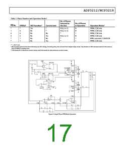
Table 4. Phase Number Configuration
PH0
PH1
Number of Phases Configured
0
1
0
1
0
0
1
1
1
1 (GPU Mode)
2
3
Multiphase operation is important for producing the high
currents and low voltages demanded by today’s microprocessors.
Handling high currents in a single-phase converter would put
too high of a thermal stress on system components such as the
inductors and MOSFETs.
In mulit-phase configuration, the timing relationship between
the phases is determined by internal circuitry that monitors the
PWM outputs. Because each phase is monitored independently,
operation approaching 100% duty cycle is possible. In addition,
more than one output can be active at a time, permitting
overlapping phases.
The multimode control of the ADP3212/NCP3218 is a stable,
high performance architecture that includes
•
•
Current and thermal balance between phases
High speed response at the lowest possible switching
frequency and minimal count of output decoupling capacitors
Minimized thermal switching losses due to lower frequency
operation
•
OPERATION MODES
The number of phases can be static (see the Number of Phases
section) or dynamically controlled by system signals to
optimize the power conversion efficiency with heavy and light
loads.
•
•
High accuracy load line regulation
High current output by supporting 2-phase or 3-phase
operation
•
•
•
Reduced output ripple due to multiphase ripple cancellation
High power conversion efficiency with heavy and light loads
Increased immunity from noise introduced by PC board
layout constraints
If ADP3212/NCP3218 is configured for mulit-phase
configuration, during a VID transient or with a heavy load
PSI
condition (indicated by DPRSLP being low and
being high),
•
•
Ease of use due to independent component selection
Flexibility in design by allowing optimization for either low
cost or high performance
the ADP3212/NCP3218 runs in multi-phase, interleaved PWM
mode to achieve minimal VCORE output voltage ripple and the best
transient performance possible. If the load becomes light
PSI
(indicated by
being low or DPRSLP being high),
NUMBER OF PHASES
ADP3212/NCP3218 switches to single-phase mode to
maximize the power conversion efficiency.
The number of operational phases can be set by the user. Tying
the PH1 pin to the GND pin forces the chip into single-phase
operation. Tying PH0 to GND and PH1 to VCC forces the chip
into 2-phase operation. Tying PH0 and PH1 to VCC forces the
chip in 3-phase operation. PH0 and PH1 should be hard wired
to VCC or GND. The ADP3212/NCP3218 switches between
single phase and multiphase operation with PSI and DPRSLP to
optimize power conversion efficiency. Table 4 summarizes PH0
and PH1.
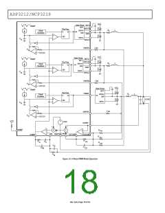
In addition to changing the number of phases, the
ADP3212/NCP3218 is also capable of dynamically changing the
control method. In dual-phase operation, the
ADP3212/NCP3218 runs in PWM mode, where the switching
frequency is controlled by the master clock. In single-phase
operation (commanded by the DPRSLP high state), the
ADP3212/NCP3218 runs in RPM mode, where the switching
frequency is controlled by the ripple voltage appearing on the
COMP pin. In RPM mode, the DRVH1 pin is driven high each
time the COMP pin voltage rises to a voltage limit set by the
VID voltage and an external resistor connected between the
RPM pin and GND. In RPM mode, the ADP3212/NCP3218
turns off the low-side (synchronous rectifier) MOSFET when
the inductor current drops to 0. Turning off the low-side
MOSFETs at the zero current crossing prevents reversed
inductor current build up and breaks synchronous operation of
Rev. SpA | Page 15 of 43

 ONSEMI [ ONSEMI ]