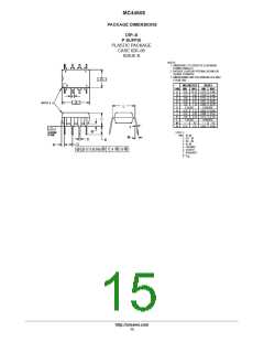
MC44608
The secondary reconfiguration is activated by the µP
applied to the secondary windings 12–14, 10–11 and 6–7
(Vaux) are thus divided by ratio N12–14 / N9–8 (number of
turns of the winding 12–14 over number of turns of the
winding 9–8). In this reconfigured status all the secondary
voltages are lowered except the 8V one. The regulation
during every pulsed or burst is performed by the zener diode
DZ3 which value has to be choosen higher than the normal
mode regulation level. This working mode creates a voltage
ripple on the 8V rail which generally must be post regulated
for the microProcessor supply.
through the switch. The dV/dt appearing on the high voltage
winding (pins 14 of the transformer) at every TMOS switch
off, produces a current spike through the series RC network
R7, C17. According to the switch position this spike is either
absorbed by the ground (switch closed) or flows into the
thyristor gate (switch open) thus firing the MCR22–6. The
closed position of the switch corresponds to the Pulsed
Mode activation. In this secondary side SMPS status the
high voltage winding (12–14) is connected through D12 and
DZ1 to the 8V low voltage secondary rail. The voltages
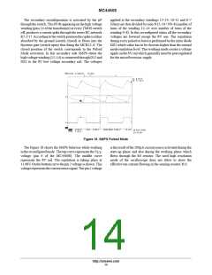
Figure 18. SMPS Pulsed Mode
The Figure 18 shows the SMPS behavior while working
is the result of the 200µA current source activated during the
start–up phase and also during the working phase which
flows through the R4 resistor. The used high resolution
mode of the oscilloscope does not allow to show the
effective ton current flowing in the sensing resistor R11.
in the reconfigured mode. The top curve represents the V
CC
voltage (pin 6 of the MC44608). The middle curve
represents the 8V rail. The regulation is taking place at
11.68V. Onthe bottom curve the pin2voltage isshown. This
voltagerepresentsthecurrentsensesignal. Thepin2voltage
http://onsemi.com
14

 ONSEMI [ ONSEMI ]