FEDL2250DIGEST-01
OKI Semiconductor
ML2252/54-XXX, ML22Q54
FUNCTIONAL DESCRIPTION
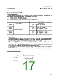
Micro-computer Interface
The micro-computer interface in the ML2250 family has 2 types of interface circuits built in: Parallel interface and
serial interface. The interface setting can be changed with the SERIAL pin.
SERIAL pin = "H" level: Serial interface
SERIAL pin = "L" level: Parallel interface
Table below shows the SERIAL pin status in the serial and parallel interfaces.
SERIAL = “L”
SERIAL = “H”
Parallel interface
Serial interface
D7 (I/O)
D6 (I/O)
D5 (I/O)
D4 (I/O)
D3 (I/O)
D2 (I/O)
D1 (I/O)
D0 (I/O)
D (I)
SCK (I)
DO (O)
D4 (I)
D3 (I)
D2 (I)
D1 (I)
D0 (I)
Serial data input pin
Serial clock input pin
Serial data output pin
Not used. (Input “L” level.)
Not used. (Input “L” level.)
Not used. (Input “L” level.)
Not used. (Input “L” level.)
Not used. (Input “L” level.)
Data input/output pins
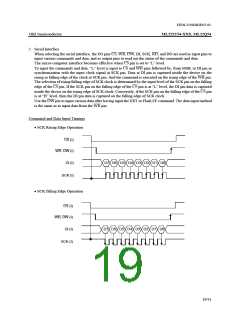
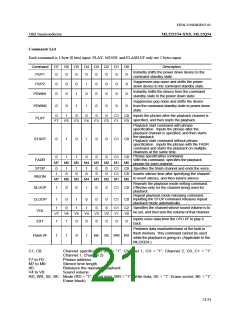
1. Parallel Interface
When selecting the parallel interface, the I/O pins CS, WR, DW, D7 to D0, and RD are used as input pins to
input various commands and data, and as output pins to read out the status of the commands and data input.
The micro-computer interface becomes effective when the CS pin is set to “L” level.
When a command or data is input, the input data to D7 through D0 pins is captured inside the device on the
rising edge of the WR pin.
The DW pin is used to input data after having input the EXT or Flash I/F command. The method to input data
to the DW pin is the same as the method to input command from the WR pin.
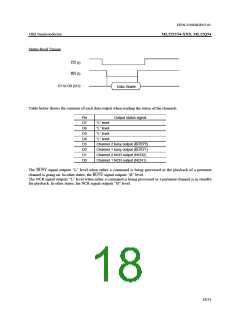
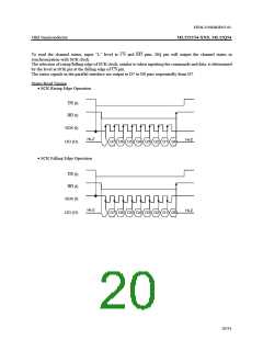
To read the channels status, pins CS and RD are made “L” level. By doing so, the status signals (NCR1, NCR2,
BUSY1, BUSY2) of each channel are output to D3 through D0 pins. D7 to D4 pins usually output “L” level.
Command and Data Input Timing
CS (I)
Data Stable
D7 to D0 (I/O)
17/31

 OKI [ OKI ELECTRONIC COMPONETS ]