FEDL2250DIGEST-01
OKI Semiconductor
ML2252/54-XXX, ML22Q54
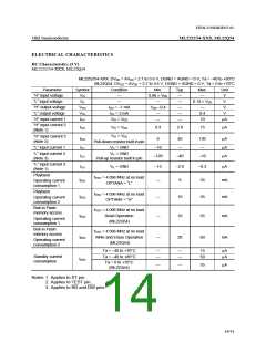
ELECTRICAL CHARACTERISTICS
DC Characteristics (3 V)
ML2252/54-XXX, ML22Q54
ML2252/54-XXX: DVDD = AVDD = 2.7 to 3.6 V, DGND = AGND = 0 V, Ta = –40 to +85°C
ML22Q54: DVDD = AVDD = 2.7 to 3.6 V, DGND = AGND = 0 V, Ta = 0 to +70°C
Parameter
“H” input voltage
“L” input voltage
“H” output voltage
“L” output voltage
“H” input current 1
Symbol
VIH
Condition
—
Min.
0.86 × VDD
—
Typ.
—
Max.
Unit
V
—
0.14 × VDD
—
VIL
—
—
V
VOH
VOL
IOH = –1 mA
IOL = 2 mA
VIH = VDD
VDD –0.4
—
—
V
—
0.4
V
IIH1
—
—
10
µA
“H” input current 2
(Note 1)
IIH2
VIH = VDD
0.3
2.0
15
µA
V
IH = VDD
“H” input current 3
(Note 2)
IIH3
IIL1
IIL2
8
40
—
130
—
µA
µA
µA
Pull-down resistor built in pin
VIL = GND
“L” input current 1
–10
–120
“L” input current 2
(Note 3)
VIL = GND
Pull-up resistor built in pin
–40
–10
“L” input current 3
(Note 1)
IIL3
VIL = GND
–15
—
–2.0
9
–0.3
35
µA
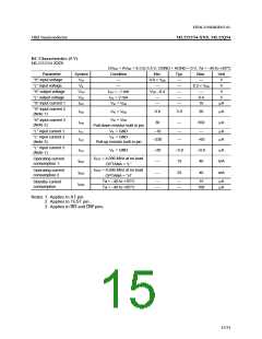
Playback
f
f
OSC = 4.096 MHz at no load
OPTANA = “L”
IDD1
mA
Operating current
consumption 1
Playback
OSC = 4.096 MHz at no load
OPTANA = “H”
IDD2
—
—
10
10
35
35
mA
mA
Operating current
consumption 2
Buit-in Flash
memory access
fOSC = 4.096 MHz at no load
Read Operation
IDD2
Operating current
consumption 1
(ML22Q54)
Buit-in Flash
memory access
fOSC = 4.096 MHz at no load
Write and Erase Operation
(ML22Q54)
IDD2
—
20
60
mA
Operating current
consumption 2
Ta = –40 to +70°C
Ta = –40 to +85°C
—
—
—
—
15
50
µA
µA
Standby current
consumption
IDDS
Ta = 0 to +70°C
(ML22Q54)
—
—
55
µA
Notes: 1. Applies to XT pin.
2. Applies to TEST pin.
3. Applies to RD and DW pins.
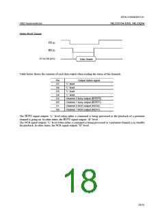
14/31

 OKI [ OKI ELECTRONIC COMPONETS ]