TJA1055
NXP Semiconductors
Enhanced fault-tolerant CAN transceiver
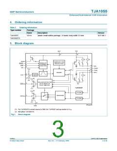
7. Functional description
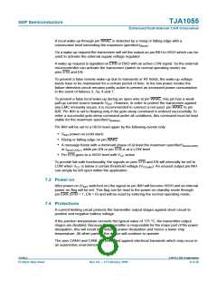
The TJA1055 is the interface between the CAN protocol controller and the physical wires
of the CAN bus (see Figure 9 and Figure 10). It is primarily intended for low-speed
applications, up to 125 kBd, in passenger cars. The device provides differential transmit
capability to the CAN bus and differential receive capability to the CAN controller.
To reduce EME, the rise and fall slopes are limited. This allows the use of an unshielded
twisted pair or a parallel pair of wires for the bus lines. Moreover, the device supports
transmission capability on either bus line if one of the wires is corrupted. The failure
detection logic automatically selects a suitable transmission mode.
In normal operating mode (no wiring failures) the differential receiver is output on pin RXD
(see Figure 1). The differential receiver inputs are connected to pins CANH and CANL
through integrated filters. The filtered input signals are also used for the single-wire
receivers. The receivers connected to pins CANH and CANL have threshold voltages that
ensure a maximum noise margin in single-wire mode.
A timer function (TxD dominant time-out function) has been integrated to prevent the bus
lines from being driven into a permanent dominant state (thus blocking the entire network
communication) due to a situation in which pin TXD is permanently forced to a LOW level,
caused by a hardware and/or software application failure.
If the duration of the LOW level on pin TXD exceeds a certain time, the transmitter will be
disabled. The timer will be reset by a HIGH level on pin TXD.
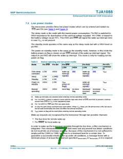
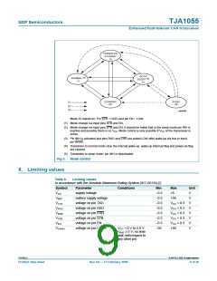
7.1 Failure detector
The failure detector is fully active in the normal operating mode. After the detection of a
single bus failure the detector switches to the appropriate mode (see Table 4). The
differential receiver threshold voltage is set at −3.2 V typical (VCC = 5 V). This ensures
correct reception with a noise margin as high as possible in the normal operating mode
and in the event of failures 1, 2, 5 and 6a. These failures, or recovery from them, do not
destroy ongoing transmissions. The output drivers remain active, the termination does not
change and the receiver remains in differential mode (see Table 4).
Failures 3, 3a and 6 are detected by comparators connected to the CANH and CANL bus
lines. Failures 3 and 3a are detected in a two-step approach. If the CANH bus line
exceeds a certain voltage level, the differential comparator signals a continuous dominant
condition. Because of inter operability reasons with the predecessor products TJA1054
and TJA1054A, after a first time-out the transceiver switches to single-wire operation
through CANH. If the CANH bus line is still exceeding the CANH detection voltage for a
second time-out, the TJA1055 switches to CANL operation; the CANH driver is switched
off and the RTH bias changes to the pull-down current source. The time-outs (delays) are
needed to avoid false triggering by external RF fields.
TJA1055_4
© NXP B.V. 2009. All rights reserved.
Product data sheet
Rev. 04 — 17 February 2009
5 of 26

 NXP [ NXP ]