TJA1055
NXP Semiconductors
Enhanced fault-tolerant CAN transceiver
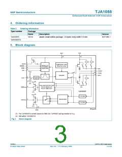
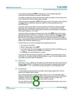
6. Pinning information
6.1 Pinning
1
2
3
4
5
6
7
14
13
12
11
10
9
INH
TXD
BAT
GND
CANL
CANH
RXD
ERR
STB
TJA1055T
TJA1055T/3
V
CC
EN
RTL
RTH
8
WAKE
001aac770
Fig 2. Pin configuration
6.2 Pin description
Table 3.
Symbol
INH
Pin description
Pin
Description
1
inhibit output for switching an external voltage regulator if a
wake-up signal occurs
TXD
RXD
ERR
2
3
4
transmit data input for activating the driver to the bus lines
receive data output for reading out the data from the bus lines
error, wake-up and power-on indication output; active LOW in
normal operating mode when a bus failure is detected; active LOW
in standby and sleep mode when a wake-up is detected; active
LOW in power-on standby when a VBAT power-on event is detected
STB
EN
5
6
standby digital control signal input; together with the input signal
on pin EN this input determines the state of the transceiver;
see Table 5 and Figure 3
enable digital control signal input; together with the input signal on
pin STB this input determines the state of the transceiver;
see Table 5 and Figure 3
WAKE
RTH
7
8
9
local wake-up signal input (active LOW); both falling and rising
edges are detected
termination resistor connection; in case of a CANH bus wire error
the line is terminated with a predefined impedance
RTL
termination resistor connection; in case of a CANL bus wire error
the line is terminated with a predefined impedance
VCC
10
11
12
13
14
supply voltage
CANH
CANL
GND
BAT
HIGH-level CAN bus line
LOW-level CAN bus line
ground
battery supply voltage
TJA1055_4
© NXP B.V. 2009. All rights reserved.
Product data sheet
Rev. 04 — 17 February 2009
4 of 26

 NXP [ NXP ]