TJA1055
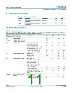
NXP Semiconductors
Enhanced fault-tolerant CAN transceiver
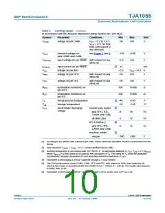
Table 8.
Static characteristics …continued
VCC = 4.75 V to 5.25 V; VBAT = 5.0 V to 40 V; VSTB = VCC; Tvj = −40 °C to +150 °C; all voltages are defined with respect to
ground; positive currents flow into the device; unless otherwise specified.[1]
Symbol
Parameter
Conditions
Min
Typ
Max
Unit
Ri(se)(CANL)
single-ended input
normal operating mode
110
165
270
kΩ
resistance on pin CANL
Ri(dif)
differential input
resistance
normal operating mode
220
330
540
kΩ
Pins RTH and RTL
Rsw(RTL) switch-on resistance on
normal operating mode; switch-on
resistance between pin RTL and
-
-
40
40
100
100
Ω
Ω
pin RTL
VCC; |IO| < 10 mA
Rsw(RTH)
switch-on resistance on
pin RTH
normal operating mode; switch-on
resistance between pin RTH and
ground; |IO| < 10 mA
VO(RTH)
IO(RTL)
Ipu(RTL)
output voltage on pin RTH low power modes; IO = 100 µA
-
0.7
1.0
−0.1
-
V
output current on pin RTL low power modes; VRTL = 0 V
−1.5
−0.65
75
mA
µA
pull-up current on pin RTL normal operating mode and
failures 4, 6 and 7
-
Ipd(RTH)
pull-down current on
pin RTH
normal operating mode and
failures 3 and 3a
-
75
-
µA
°C
Thermal shutdown
Tj(sd) shutdown junction
temperature
160
175
190
[1] All parameters are guaranteed over the virtual junction temperature range by design, but only 100 % tested at Tamb = 125 °C for dies on
wafer level, and above this for cased products 100 % tested at Tamb = 25 °C, unless otherwise specified.
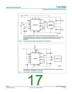
11. Dynamic characteristics
Table 9.
Dynamic characteristics
VCC = 4.75 V to 5.25 V; VBAT = 5.0 V to 40 V; VSTB = VCC; Tvj = −40 °C to +150 °C; all voltages are defined with respect to
ground; unless otherwise specified.[1]
Symbol
Parameter
Conditions
Min Typ Max Unit
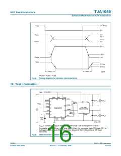
tt(reces-dom) transition time for recessive to
dominant (on pins CANL and
CANH)
between 10 % and 90 %; RCAN_L = RCAN_H
125 Ω; CCAN_L = CCAN_H = 1 nF;
see Figure 5 and 6
=
=
0.2 0.6
-
µs
tt(dom-reces) transition time for dominant to
recessive (on pins CANL and
CANH)
between 10 % and 90 %; RCAN_L = RCAN_H
125 Ω; CCAN_L = CCAN_H = 1 nF;
see Figure 5 and 6
0.3 0.7
-
µs
tPD(L)
propagation delay TXD (LOW) to
RXD (LOW)
no failures; RCAN_L = RCAN_H = 125 Ω;
-
-
-
-
-
-
1.5 µs
1.9 µs
1.9 µs
CCAN_L = CCAN_H = 1 nF; see Figure 4 to
Figure 6
all failures except CAN_L shorted to CAN_H;
RCAN_L = RCAN_H = 125 Ω; CCAN_L
CAN_H = 1 nF; see Figure 4 to Figure 6
=
C
failure 7, CAN_L shorted to CAN_H;
RCAN_L = 1 MΩ; RCAN_H = 125 Ω;
CCAN_L = CCAN_H = 1 nF; see Figure 4 to
Figure 6
TJA1055_4
© NXP B.V. 2009. All rights reserved.
Product data sheet
Rev. 04 — 17 February 2009
14 of 26

 NXP [ NXP ]