TJA1055
NXP Semiconductors
Enhanced fault-tolerant CAN transceiver
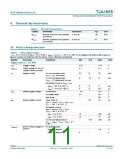
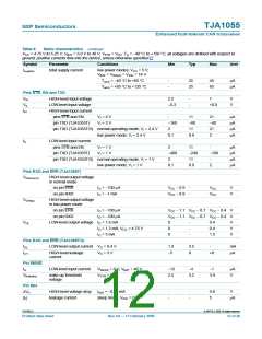
Table 8.
Static characteristics …continued
VCC = 4.75 V to 5.25 V; VBAT = 5.0 V to 40 V; VSTB = VCC; Tvj = −40 °C to +150 °C; all voltages are defined with respect to
ground; positive currents flow into the device; unless otherwise specified.[1]
Symbol
Parameter
Conditions
Min
Typ
Max
Unit
Isup(tot)
total supply current
low power modes; VCC = 5 V;
V
BAT = VWAKE = VINH = 14 V
Tamb = −40 °C to +85 °C
Tamb = +85 °C to +125 °C
-
-
25
25
45
65
µA
µA
Pins STB, EN and TXD
VIH
VIL
IIH
HIGH-level input voltage
2.2
-
-
7
V
V
LOW-level input voltage
HIGH-level input current
pins STB and EN
−0.3
+0.8
VI = 4 V
VI = 3 V
-
11
21
−40
21
2
µA
µA
µA
µA
pin TXD (TJA1055T)
−160
2
−80
11
pin TXD (TJA1055T/3) normal operating mode; VI = 2.4 V
low power mode; VI = 2.4 V
0.1
0.9
IIL
LOW-level input current
pins STB and EN
VI = 1 V
VI = 1 V
2
11
-
µA
µA
µA
µA
pin TXD (TJA1055T)
−400
2
−240
11
−100
pin TXD (TJA1055T/3) normal operating mode; VI = 1 V
low power mode; VI = 1 V
-
0.1
0.9
2
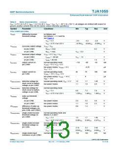
Pins RXD and ERR (TJA1055T)
VOH(norm) HIGH-level output voltage
in normal mode
on pin ERR
IO = −100 µA
IO = −1 mA
V
CC − 0.9
-
-
VCC
VCC
V
V
on pin RXD
V
CC − 0.9
VOH(lp)
HIGH-level output voltage
in low-power mode
on pin ERR
on pin RXD
IO = −100 µA
IO = −100 µA
V
V
0
0
0
CC − 1.1
V
V
-
CC − 0.7
CC − 0.7
V
CC − 0.4
CC − 0.4
V
V
V
V
V
CC − 1.1
V
VOL
LOW-level output voltage IO = 1.6 mA
IO = 1.2 mA; VCC < 4.75 V
IO = 5 mA
0.4
0.4
1.5
-
-
Pins RXD and ERR (TJA1055T/3)
IOL
ILH
LOW-level output current VO = 0.4 V
1.3
3.5
0
-
mA
HIGH-level leakage
current
VO = 3 V
−5
+8
µA
Pin WAKE
IIL
LOW-level input current
VWAKE = 0 V; VBAT = 40 V
VSTB = 0 V
−12
−4
−1
µA
Vth(wake)
wake-up threshold
voltage
2.5
3.2
3.9
V
Pin INH
∆VH
HIGH-level voltage drop
leakage current
IINH = −0.18 mA
-
-
-
-
0.8
5
V
|IL|
sleep mode; VINH = 0 V
µA
TJA1055_4
© NXP B.V. 2009. All rights reserved.
Product data sheet
Rev. 04 — 17 February 2009
12 of 26

 NXP [ NXP ]