TJA1055
NXP Semiconductors
Enhanced fault-tolerant CAN transceiver
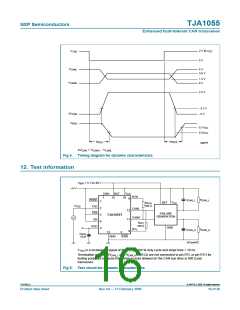
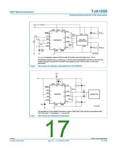
V
BAT
= 5 V to 40 V
+5 V
V
INH
BAT
14
CC
RTH
1
10
8
C
CAN_L
R
CAN_L
WAKE
7
2
5
6
3
BAT
V
CC
R
RTH
500 Ω
V
TXD
TXD
STB
CANL
CANH
12
11
+3.3 V
FAILURE
GENERATION
TJA1055T/3
EN
2.5
kΩ
R
RTL
500 Ω
RXD
GND
RTL
C
CAN_H
R
CAN_H
9
4
13
GND
C
RXD
10 pF
ERR
001aac933
VTXD is a rectangular signal of 50 kHz with 50 % duty cycle and slope time < 10 ns.
Termination resistors RCAN_L and RCAN_H (125 Ω) are not connected to pin RTL or pin RTH for
testing purposes because the minimum load allowed on the CAN bus lines is 500 Ω per
transceiver.
Fig 6. Test circuit for dynamic characteristics (TJA1055T/3)
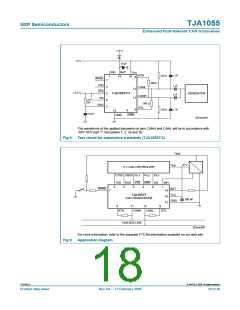
+12 V
+5 V
10 µF
V
INH
BAT
14
CC
8
RTH
1 nF
125 Ω
1
10
WAKE
7
2
5
6
3
500 Ω
TXD
STB
1 nF
1 nF
CANL
CANH
12
11
TJA1055T
GENERATOR
EN
500 Ω
RXD
RTL
9
125 Ω
1 nF
4
13
GND
10 pF
ERR
001aac934
The waveforms of the applied transients on pins CANH and CANL will be in accordance with
“ISO 7637 part 1”: test pulses 1, 2, 3a and 3b.
Fig 7. Test circuit for automotive transients
TJA1055_4
© NXP B.V. 2009. All rights reserved.
Product data sheet
Rev. 04 — 17 February 2009
17 of 26

 NXP [ NXP ]