TDF8544
NXP Semiconductors
I2C-bus controlled 4 50 W power amplifier
7. Functional description
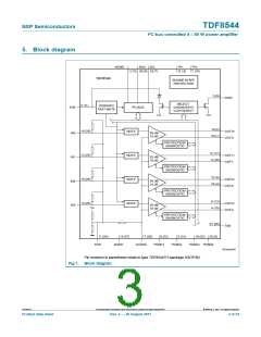
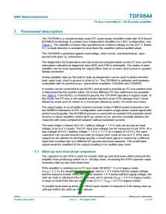
The TDF8544 is a complementary quad BTL audio power amplifier made with SOI-based
BCDMOS technology. It contains four independent amplifiers in a BTL configuration; see
Figure 1. The amplifier remains fully operational at a battery voltage as low as 6 V. Below
6 V, a crank detector is activated to shut down the amplifier without audible plops.
The TDF8544 is protected against overvoltage, short-circuit, overtemperature, open
ground and open VP connections.
The diagnostics for temperature and clip levels are programmable via the I2C-bus, and the
information indicated at diagnostic pins DIAG and STB is selectable. The status of each
amplifier can be read separately for output offset, load or no load, short-circuit or speaker
falsely connected.
During amplifier start-up the built-in start-up diagnostics can be used to detect shorted
load, open load, short to ground or short to VP. The TDF8544 is software and hardware
compatible with its predecessors: stand-alone amplifiers TDA8594 and TDA8595.
A resistor can be connected to pin ADSEL and ground to emulate an I2C-bus address that
is determined by the resistor value. Up to four different I2C-bus addresses are possible;
see Table 8. If pin ADSEL is shorted to ground, the TDF8544 operates in legacy mode. In
this mode, the I2C-bus is not needed and the function of pin STB changes from 2-level
(Stand-by mode and On mode) to a 3-level pin (Stand-by mode, On mode and mute).
The output stage of an amplifier channel consists of two PDMOS power transistors and
two NDMOS transistors in BTL configuration and ensures a high power output signal with
perfect sound quality. The BCDMOS process is used with an isolated SOI substrate which
ensures a robust amplifier, where latch-up cannot occur, and low crosstalk between the
channels with every component isolated, without substrate currents.
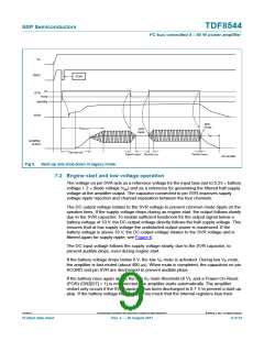
The input stage is biased (at 0.23 battery voltage + 1.4 V) and can accept an input
voltage of up to 8 V (peak). The DC input bias voltage can be measured on pin SVR. At a
bias voltage of 0.23 battery voltage + 1.4 V (= 4.7 V at a supply of 14.4 V), the input
capacitors can remain biased even with an engine start crank as low as 6 V. If the input
capacitors are allowed to discharge quickly, a small input signal is caused by a different
input time-constant due to a different AC ground and input capacitor. This small input
signal would be amplified to the output resulting in an audible plop noise.
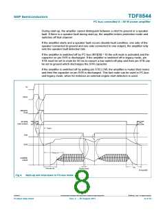
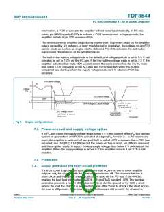
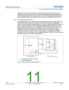
7.1 Start-up and shut-down sequence
The capacitor on pin SVR is used for smooth start-up and shut-down which prevents the
amplifier from producing switch-on or -off plop noise. Increasing the SVR capacitor value
increases start-up and shut-down time.
If the amplifier is switched on in I2C-bus mode (IB1[D0] = 1) or in legacy mode
(VSTB > 2.5 V), the amplifier output voltage rises to 1.4 V below half the supply voltage
and the output is muted. When the output reaches 1.4 V below half the supply voltage, the
start-up mute is released if the I2C-bus was set to unmute (VSTB > 5.9 V in legacy mode),
or stays in mute if the bits are set to mute (2.5 V < VSTB < 4.5 V in legacy mode).
To enable short start-up times, the 70 k input resistor is reduced to 3 k during start-up
until just before the start-up mute release.
TDF8544
All information provided in this document is subject to legal disclaimers.
© NXP B.V. 2011. All rights reserved.
Product data sheet
Rev. 2 — 29 August 2011
7 of 54

 NXP [ NXP ]