TDF8544
NXP Semiconductors
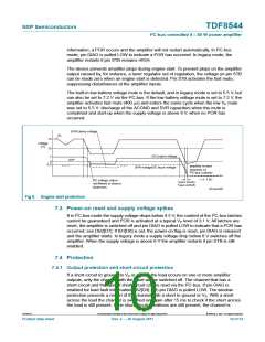
I2C-bus controlled 4 50 W power amplifier
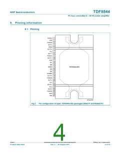
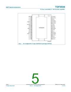
6.2 Pin description
Table 3.
Symbol Pin
TDF8544J/SD
Pin description
Description
TDF8544TH
ADSEL
STB
1
10
11
I2C-bus address select
stand-by (I2C-bus mode) or mode pin (legacy mode)
programmable second clip indicator
2
PGND2
OUT2
DIAG
OUT2+
VP2
3
14
15
9
channel 2 power ground
4
channel 2 negative output (right rear)
diagnostic and clip detection output
channel 2 positive output (right rear)
power supply voltage 2
5
6
13
16
18
23
17
24
25
26
27
28
29
30
2
7
OUT1
PGND1
OUT1+
SVR
8
channel 1 negative output (right front)
channel 1 power ground
9
10
11
12
13
14
15
16
channel 1 positive output (right front)
half supply voltage filter capacitor
channel 1 input
IN1
IN2
channel 2 input
SGND
IN4
signal ground
channel 4 input
IN3
channel 3 input
ACGND 17
AC ground
OUT3+
PGND3
OUT3
VP1
18
19
20
21
22
23
24
25
26
27
-
channel 3 positive output (left front)
channel 3 power ground
32
1
channel 3 negative output (left front)
power supply voltage 1
3
OUT4+
SCL
6
channel 4 positive output (left rear)
I2C-bus clock input
7
OUT4
PGND4
SDA
4
channel 4 negative output (left rear)
5
channel 4 power ground
8
I2C-bus data input and output
heatsink connection; must be connected to ground
not connected
TAB
36
n.c.
12, 19, 20,
21, 22, 31,
33, 34, 35
TDF8544
All information provided in this document is subject to legal disclaimers.
© NXP B.V. 2011. All rights reserved.
Product data sheet
Rev. 2 — 29 August 2011
6 of 54

 NXP [ NXP ]