TDF8544
NXP Semiconductors
I2C-bus controlled 4 50 W power amplifier
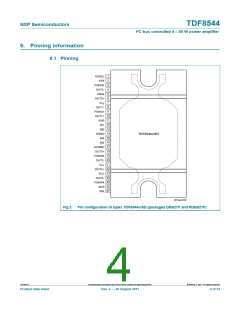
6. Pinning information
6.1 Pinning
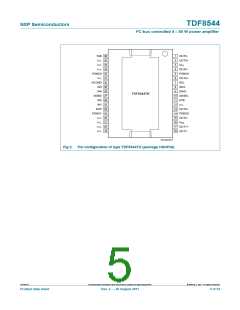
1
ADSEL
STB
2
3
PGND2
OUT2-
DIAG
4
5
6
OUT2+
7
V
P2
8
OUT1-
PGND1
OUT1+
SVR
9
10
11
12
13
14
15
16
17
18
19
20
21
22
23
24
25
26
27
IN1
IN2
SGND
IN4
TDF8544J/SD
IN3
ACGND
OUT3+
PGND3
OUT3-
V
P1
OUT4+
SCL
OUT4-
PGND4
SDA
TAB
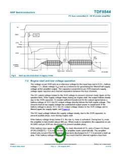
001aan046
Fig 2. Pin configuration of types TDF8544J/SD (packages DBS27P and RDBS27P)
TDF8544
All information provided in this document is subject to legal disclaimers.
© NXP B.V. 2011. All rights reserved.
Product data sheet
Rev. 2 — 29 August 2011
4 of 54

 NXP [ NXP ]