TDF8544
NXP Semiconductors
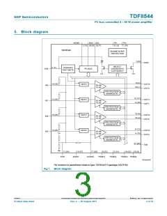
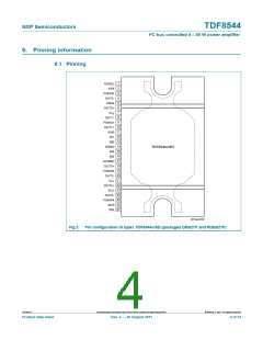
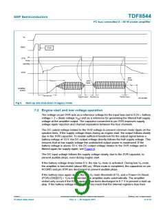
I2C-bus controlled 4 50 W power amplifier
Temperature controlled gain reduction to prevent audio holes at high junction
temperatures
Programmable low battery voltage detection to enable 7.5 V or 6 V minimum battery
voltage operation
Overvoltage protection (load-dump safe up to VP = 50 V) with overvoltage pre-warning
at 16 V
Offset detection
3. Quick reference data
Table 1.
Quick reference data
Symbol Parameter
Conditions
Min
Typ
Max
Unit
VP(oper) operating supply
voltage
RL = 4
6
14.4
18
V
Iq
quiescent current
no load
-
260
190
22
350
mA
mA
W
no load; VP = 7 V
-
-
Po
output power
RL = 4 ; VP = 14.4 V; THD = 0.5 %
RL = 4 ; VP = 14.4 V; THD = 10 %
RL = 2 ; VP = 14.4 V; THD = 10 %
RL = 4 ; VP = 15.2 V; Vi = 2 V RMS square wave
RL = 2 ; VP = 14.4 V; Vi = 2 V RMS square wave
Po = 1 W to 12 W; fi = 1 kHz; RL = 4
19
26
45
47
70
-
-
28
-
W
51
-
W
maximum output
power
50
-
W
Po(max)
75
-
W
THD
Vn(o)
total harmonic
distortion
0.01
0.1
%
output noise voltage filter 20 Hz to 22 kHz (6th order); RS = 50
amplifier mode
line driver mode
-
-
40
25
60
33
V
V
4. Ordering information
Table 2.
Ordering information
Type number
Package
Name
Description
Version
TDF8544J/N2
TDF8544SD/N2
TDF8544TH/N2
DBS27P
plastic DIL-bent-SIL (special bent) power package; 27 leads (lead length
6.8 mm)
SOT827-1
RDBS27P
HSOP36
plastic rectangular-DIL-bent-SIL (reverse bent) power package; 27 leads SOT878-1
(row spacing 2.54 mm)
plastic, heatsink small outline package; 36 leads; low stand-off height
SOT851-1
TDF8544
All information provided in this document is subject to legal disclaimers.
© NXP B.V. 2011. All rights reserved.
Product data sheet
Rev. 2 — 29 August 2011
2 of 54

 NXP [ NXP ]