TDA8950
NXP Semiconductors
2 × 150 W class-D power amplifier
13. Application information
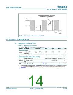
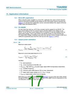
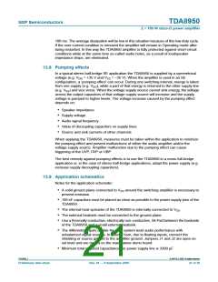
13.1 Mono BTL application
When using the power amplifier in a mono BTL application the inputs of both channels
must be connected in parallel and the phase of one of the inputs must be inverted (see
Figure 7). In principle the loudspeaker can be connected between the outputs of the two
single-ended demodulation filters.
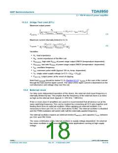
13.2 Pin MODE
For pop noise-free start-up, an RC time-constant must be applied on pin MODE. The
bias-current setting of the VI-converter input is directly related to the voltage on pin
MODE. In turn the bias-current setting of the VI converters is directly related to the DC
output offset voltage. Thus a slow dV/dt on pin MODE results in a slow dV/dt for the
DC output offset voltage, resulting in pop noise-free start-up. A time-constant of 500 ms is
sufficient to guarantee pop noise-free start-up (see also Figure 4, 5 and 8).
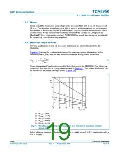
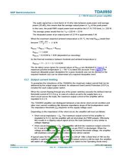
13.3 Output power estimation
13.3.1 SE
Maximum output power:
2
R
L
× V × (1 – t
× 0.5 f
)
osc
----------------------------------------------------
P
min
R + R
+ R
sL
L
DSon(hs)
P
=
(1)
(2)
---------------------------------------------------------------------------------------------------------------------------------
2R
o(0.5%)
L
Maximum current internally limited to 9.2 A:
V × (1 – t
× 0.5 f
)
osc
P
min
I
=
-------------------------------------------------------------
R + R + R
o(peak)
L
DSon(hs)
sL
Variables:
• RL: load impedance
• RsL: series impedance of the filter coil
• RDSon(hs): high-side RDSon of power stage output DMOS (temperature dependent)
• fosc: oscillator frequency
• tmin: minimum pulse width (typical 150 ns, temp. dependent)
• VP: single-sided supply voltage (or 0.5 × (VDD + |VSS|))
• Po(0.5 %): output power at the onset of clipping
Note that Io(peak) should be below 9.2 A (Section 8.3.2). Io(peak)M is the sum of the current
through the load and the ripple current. The value of the ripple current is dependent on the
coil inductance and voltage drop over the coil.
TDA8950_1
© NXP B.V. 2008. All rights reserved.
Preliminary data sheet
Rev. 01 — 9 September 2008
17 of 39

 NXP [ NXP ]