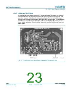
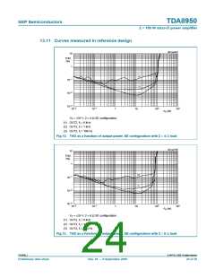
TDA8950
NXP Semiconductors
2 × 150 W class-D power amplifier
100 ms. The average dissipation will be low in this situation because of this low duty cycle.
If the over current condition is removed the amplifier will remain in Operating mode after
being restarted. In this way the TDA8950 amplifier is fully protected against short-circuit
conditions while at the same time so-called audio holes, as a result of loudspeaker
impedance drops, are eliminated.
13.8 Pumping effects
In a typical stereo half-bridge SE application the TDA8950 is supplied by a symmetrical
voltage (e.g. VDD = +35 V and VSS = −35 V). When the amplifier is used in an SE
configuration, a ‘pumping effect’ can occur. During one switching interval, energy is taken
from one supply (e.g. VDD), while a part of that energy is returned to the other supply line
(e.g. VSS) and vice versa. When the voltage supply source cannot sink energy, the voltage
across the output capacitors of that voltage supply source will increase and the supply
voltage is pumped to higher levels. The voltage increase caused by the pumping effect
depends on:
• Speaker impedance
• Supply voltage
• Audio signal frequency
• Value of decoupling capacitors on supply lines
• Source and sink currents of other channels
When applying the TDA8950, measures must be taken within the application to minimize
the pumping effect and prevent malfunctions of either the audio amplifier and/or the
voltage supply source. Amplifier malfunction due to the pumping effect can cause
triggering of the UVP, OVP or UBP.
The best remedy against pumping effects is to use the TDA8950 in a mono full-bridge
application or, in the case of stereo half-bridge applications, adapt the power supply (e.g.
increase supply decoupling capacitors).
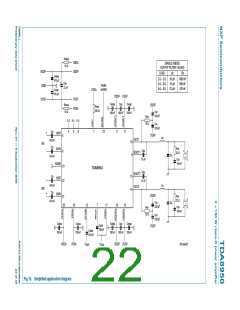
13.9 Application schematics
Notes for the application schematic:
• A solid ground plane connected to VSS around the switching amplifier is necessary to
prevent emission.
• 100 nF capacitors must be placed as close as possible to the power supply pins of the
TDA8950.
• The internal heat spreader of the TDA8950 is internally connected to VSS
.
• The external heatsink must be connected to the ground plane.
• Use a thermally conductive, electrically non-conductive, Sil-Pad between the backside
of the TDA8950 and a small external heatsink.
• The differential inputs enable the best system level audio performance with
unbalanced signal sources. In case of hum, due to floating inputs, connect the
shielding or source ground to the amplifier ground. Jumpers J1 and J2 are open on
set level and are closed on the stand-alone demo board.
• Minimum total required capacitance per power supply line is 3300 µF.
TDA8950_1
© NXP B.V. 2008. All rights reserved.
Preliminary data sheet
Rev. 01 — 9 September 2008
21 of 39

 NXP [ NXP ]