TDA8950
NXP Semiconductors
2 × 150 W class-D power amplifier
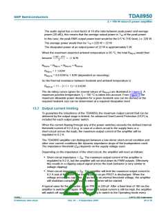
12.3 Mono BTL application characteristics
Table 10. Dynamic characteristics
VP = ±35 V; RL = 8 Ω; fi = 1 kHz; fosc = 345 kHz; RsL < 0.1 Ω [1]; Tamb = 25 °C; unless otherwise
specified.
Symbol Parameter
Conditions
Min
Typ
Max Unit
[2]
Po
output power
L = 22 µH; C = 680 nF;
Tj = 85 °C; RL = 8 Ω
THD = 10 %; VP = ±39 V
THD = 10 %; VP = ±37 V
THD = 0.5 %; VP = ±37 V
Po = 1 W; fi = 1 kHz
-
-
-
-
-
-
340
300
200
0.05
0.05
36
-
-
-
-
-
-
W
W
W
%
%
dB
[3]
[3]
THD
total harmonic
distortion
Po = 1 W; fi = 6 kHz
Gv(cl)
closed-loop voltage
gain
SVRR
supply voltage ripple
rejection
between pin VDDPn and
SGND
[4]
[4]
[4]
[4]
operating; fi = 100 Hz
operating; fi = 1 kHz
mute; fi = 100 Hz
-
-
-
-
80
-
-
-
-
dB
dB
dB
dB
80
95
standby; fi = 100 Hz
120
between pin VSSPn and
SGND
[4]
[4]
[4]
[4]
operating; fi = 100 Hz
operating; fi = 1 kHz
mute; fi = 100 Hz
-
75
75
90
130
63
-
-
-
-
-
dB
dB
dB
dB
kΩ
-
-
standby; fi = 100 Hz
-
Zi
input impedance
measured between the input
pins and SGND
45
[5]
[6]
[7]
Vn(o)
output noise voltage
operating; Rs = 0 Ω
mute
-
-
-
-
190
45
-
-
-
-
µV
µV
dB
dB
αmute
mute attenuation
fi = 1 kHz; Vi = 2 V (RMS)
Vi(CM) = 1 V (RMS)
82
CMRR common mode
rejection ratio
75
[1] RsL is the series resistance of inductor of low-pass LC filter in the application.
[2] Output power is measured indirectly; based on RDSon measurement. See also Section 13.3.
[3] Total harmonic distortion is measured in a bandwidth of 22 Hz to 20 kHz, using an AES17 20 kHz brickwall
filter. Maximum limit is guaranteed but may not be 100 % tested.
[4] Vripple = Vripple(max) = 2 V (p-p); Rs = 0 Ω.
[5] B = 22 Hz to 20 kHz, using an AES17 20 kHz brickwall filter. Low noise due to BD modulation.
[6] B = 22 Hz to 20 kHz, using an AES17 20 kHz brickwall filter; independent of Rs.
[7] Vi = Vi(max) = 1 V (RMS); fi = 1 kHz.
TDA8950_1
© NXP B.V. 2008. All rights reserved.
Preliminary data sheet
Rev. 01 — 9 September 2008
16 of 39

 NXP [ NXP ]