Philips Semiconductors
Product specication
I2C-bus controlled 4 45 Watt power
amplier and multiple voltage regulator
TDA8589J; TDA8589xJ
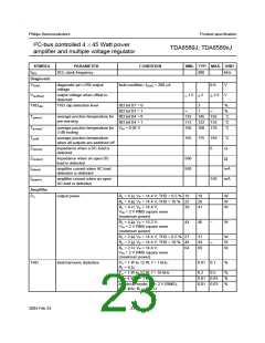
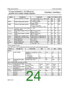
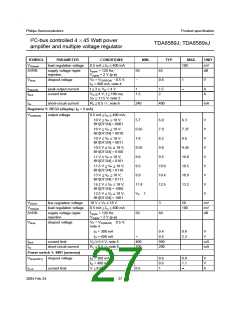
SYMBOL
PARAMETER
CONDITION
MIN. TYP. MAX. UNIT
channel separation (crosstalk)
f = 1 Hz to 10 kHz; Rsource = 600
Po = 4 W; f = 1 kHz
50
60
80
70
dB
dB
dB
cs
SVRR
CMRR
supply voltage ripple rejection
common mode ripple rejection
f = 100 Hz to 10 kHz;
Rsource = 600
55
40
amplier mode;
70
dB
Vcommon = 0.3 V (p-p);
f = 1 kHz to 3 kHz; Rsource = 0
Vcm(max)(rms) maximum common mode voltage f = 1 kHz
level (rms value)
0.6
35
70
V
V
V
Vn(o)(LN)
noise output voltage in line driver lter 20 Hz to 22 kHz;
25
50
mode
Rsource = 600
Vn(o)(amp)
noise output voltage in amplier
lter 20 Hz to 22 kHz;
mode
Rsource = 600
Gv(amp)
Gv(LN)
Zi
voltage gain in amplier mode
voltage gain in line driver mode
input impedance
single-ended in to differential out
single-ended in to differential out
CIN = 220 nF
25
19
55
80
26
20
70
90
70
20
27
21
dB
dB
k
mute attenuation
VO(on)/VO(mute)
dB
V
mute
Vo(mute)
output voltage mute
VIN = 1 V (RMS)
Bp
power bandwidth
1 dB; THD = 1 %
kHz
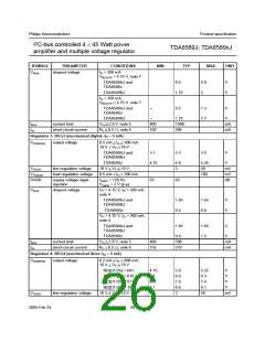
Voltage regulator section
Tamb = 25 C; VP = 14.4 V; measured in the test circuit Fig.28; unless otherwise specied.
SYMBOL
PARAMETER
CONDITIONS
MIN.
TYP.
MAX.
UNIT
Supply
VP
supply voltage
regulator 1, 3, 4 and 5 on 10.0
regulator 2
14.4
18
V
switched on
in regulation
4
V
V
V
A
6.3
50
overvoltage for shut-down 18.1
standby mode; note 1
22
Iq(tot)
total quiescent supply
current
150
190
Reset output (push-pull stage, pin RST)
VREG2(th)(r) rising threshold voltage
of regulator 2
VP is rising;
IO(REG2) = 50 mA
VO(REG2)
0.2
VO(REG2)
0.1
VO(REG2)
0.04
V
V
VREG2(th)(f) falling threshold voltage VP is falling;
VO(REG2)
0.25
VO(REG2)
0.15
VO(REG2)
0.1
of regulator 2
IO(REG2) = 50 mA
Isink(L)
LOW-level sink current
VRST 0.8 V
1
mA
A
Isource(H)
HIGH-level source
current
VRST = VO(REG2) 0.5 V;
VP = 14.4 V
200
600
tr
tf
rise time
fall time
note 2
note 2
2
50
50
s
s
10
2004 Feb 24
24

 NXP [ NXP ]