Philips Semiconductors
Product specication
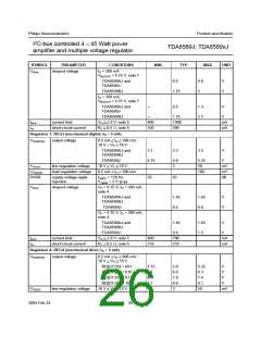
I2C-bus controlled 4 45 Watt power
amplier and multiple voltage regulator
TDA8589J; TDA8589xJ
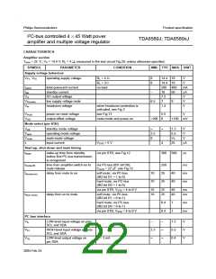
CHARACTERISTICS
Amplier section
Tamb = 25 C; VP = 14.4 V; RL = 4 ; measured in the test circuit Fig.28; unless otherwise specied.
SYMBOL PARAMETER CONDITION MIN. TYP. MAX. UNIT
Supply voltage behaviour
VP1, VP2
operating supply voltage
RL = 4
RL = 2
no load
8
8
14.4 18
14.4 16
280 400
V
V
Iq(tot)
Istb
total quiescent current
standby current
mA
A
10
7.2
7
50
VO
DC output voltage
low supply voltage mute
headroom voltage
V
VP(mute)
Vhr
6.5
8
V
when headroom protection is
activated; see Fig.3
1.4
V
VPOR
VOO
power-on reset voltage
output offset voltage
see Fig.13
5.5
0
V
mute mode and power on
100
+100 mV
Mode select (pin STB)
Vstb
Voper
Vmute
II
standby mode voltage
1.3
5.5
VP
25
V
V
V
operating mode voltage
mute mode voltage
input current
2.5
8
VSTB = 5 V
4
A
Start-up, shut-down and mute timing
twake
wake-up time from standby
before rst I2C-bus transmission
is recognised
via pin STB; see Fig.12
300 500
250
s
tmute(off)
time from amplier switch-on to
mute release
via I2C-bus (IB1 bit D0);
CSVR = 22 F; see Fig.12
soft mute; via I2C-bus
(IB2 bit D1 = 1 to 0)
hard mute; via I2C-bus
(IB2 bit D0 = 1 to 0)
ms
ms
ms
td(mute-on)
delay from mute to on
10
10
25
25
40
40
via pin STB; VSTB = 4 to 8 V
soft mute; via I2C-bus
(IB2 bit D1 = 0 to 1)
10
10
25
25
40
40
ms
ms
td(on-mute)
delay from on to mute
hard mute; via I2C-bus
(IB2 bit D0 = 0 to 1)
0.4
0.4
1
1
ms
ms
via pin STB; VSTB = 4 to 8 V
I2C-bus interface
VIL
LOW-level input voltage on pins
SCL and SDA
1.5
5.5
0.4
V
V
V
VIH
VOL
HIGH-level input voltage on pins
SCL and SDA
2.3
LOW-level output voltage on
pin SDA
IL = 3 mA
2004 Feb 24
22

 NXP [ NXP ]