Philips Semiconductors
Product specication
I2C-bus controlled 4 45 Watt power
amplier and multiple voltage regulator
TDA8589J; TDA8589xJ
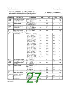
SYMBOL
fSCL
PARAMETER
CONDITION
MIN. TYP. MAX. UNIT
SCL clock frequency
400
kHz
Diagnostic
VDIAG
diagnostic pin LOW output
voltage
fault condition; IDIAG = 200 A
0.8
2.5
V
V
Vo(offset)
THDclip
output voltage when offset is
detected
1.5
2
THD clip detection level
IB3 bit D7 = 0
IB3 bit D7 = 1
3
1
%
%
C
C
C
Tj(warn)
average junction temperature for IB3 bit D4 = 0
pre-warning
135
145 155
122 132
160 170
IB3 bit D4 = 1
112
150
Tj(mute)
Tj(off)
average junction temperature for VIN = 0.05 V
3 dB muting
average junction temperature
when all outputs are switched off
165
175 185
6
C
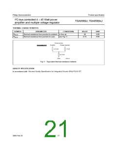
Zo(load)
Zo(open)
Io(load)
Io(open)
impedance when a DC load is
detected
impedance when an open DC
load is detected
500
550
amplier current when AC load
detection is detected
mA
mA
amplier current when an open
150
AC load is detected
Amplier
Po
output power
RL = 4 ; VP = 14.4 V; THD = 0.5 % 18
RL = 4 ; VP = 14.4 V; THD = 10 % 25
19
26
41
W
W
W
RL = 4 ; VP = 14.4 V;
VIN = 2 V RMS square wave
(maximum power)
39
RL = 4 ; VP = 15.2 V;
VIN = 2 V RMS square wave
(maximum power)
44
46
W
RL = 2 ; VP = 14.4 V; THD = 0.5 % 27
RL = 2 ; VP = 14.4 V; THD = 10 % 40
31
44
69
W
W
W
RL = 2 ; VP = 14.4 V;
VIN = 2 V RMS square wave
(maximum power)
64
THD
total harmonic distortion
Po = 1 W to 12 W; f = 1 kHz;
RL = 4
0.01 0.1
%
Po = 1 W to 12 W; f = 10 kHz
Po = 4 W; f = 1 kHz
0.2
0.5
%
%
%
0.01 0.03
0.01 0.03
line driver mode; Vo = 2 V (RMS);
f = 1 kHz; RL = 600
2004 Feb 24
23

 NXP [ NXP ]