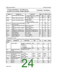
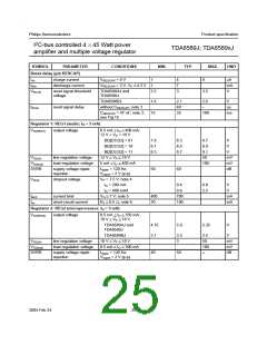
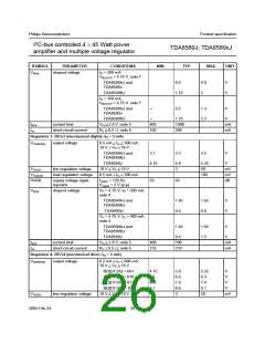
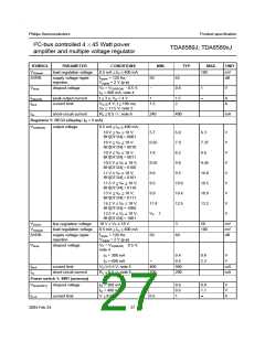
Philips Semiconductors
Product specication
I2C-bus controlled 4 45 Watt power
amplier and multiple voltage regulator
TDA8589J; TDA8589xJ
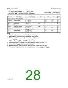
SYMBOL
PARAMETER
CONDITIONS
MIN.
TYP.
MAX.
UNIT
Power switch 2: SW2 (amplier)
Vdrop(SW2) dropout voltage
IO = 300 mA
0.6
0.6
1
0.8
1.1
V
V
A
IO = 400 mA
VO 8.5 V
Ilimit
current limit
0.5
0.4
Backup switch
IDC(BU)
continuous current
VBUCAP 6 V
1.5
24
A
V
Vclamp(BU) clamping voltage
VP = 30 V;
28
IO(REG2) = 100 mA
Vdrop
dropout voltage
IO = 500 mA;
0.6
0.8
V
(VP VBUCAP
)
Notes
1. The quiescent current is measured in standby mode when RL =
2. The rise and fall times are measured with a 50 pF load capacitor.
.
3. The reset delay time depends on the value of the reset delay capacitor:
CRESCAP
td rst
=
V th rst = CRESCAP 750 103
s
------------------------
Ich
4. The dropout voltage of a regulator is the voltage difference between VP and VO(REGn)
.
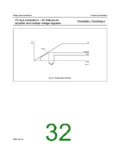
5. At current limit, VO(REGn) is held constant (see Fig.6).
6. The foldback current protection limits the dissipation power at short-circuit (see Fig.6).
7. The dropout voltage of regulator 2 is the voltage difference between VBUCAP and VO(REG2)
.
2004 Feb 24
28

 NXP [ NXP ]