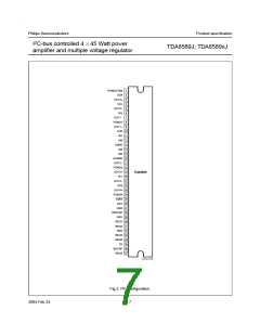
Philips Semiconductors
Product specication
I2C-bus controlled 4 45 Watt power
amplier and multiple voltage regulator
TDA8589J; TDA8589xJ
VOLTAGE REGULATORS
Backup function
The voltage regulator section contains:
The backup function is implemented by a switch function,
which behaves like an ideal diode between pins VP
and BUCAP; the forward voltage of this ideal diode
depends on the current flowing through it. The backup
function supplies regulator 2 during brief periods when no
supply voltage is present on pin VP. It requires an external
capacitor to be connected to pin BUCAP and ground.
When the supply voltage is present on pin VP this
Four switchable regulators and one permanent active
regulator
Two power switches with loss-of-ground protection
Reset push-pull output
Backup functionality.
The quiescent current condition has a very low current
level of 150 A typical with only regulator 2 active. The
TDA8589 uses low dropout voltage regulators for use in
low voltage applications.
capacitor will be charged to a level of VP 0.3 V. When the
supply voltage is absent from pin VP, this charge can then
be used to supply regulator 2 for a brief period (tbackup
calculated using the formula:
)
All of the voltage regulators except for the standby
regulator can be controlled via the I2C-bus. The voltage
regulator section of this device has two power switches
which are capable of delivering unregulated 400 mA
continuous current, and has several fail-safe protection
modes. It conforms to peak transient tests and protects
against continuous high voltage (24 V), short-circuits and
thermal stress. A reset warning signal is asserted if
regulator 2 is out of regulation. Regulator 2 will try to
maintain output for as long as possible even if a thermal
shut-down or any other fault condition occurs. During
overvoltage stress conditions, all outputs except
V
P – V
– 0.5
---------------------O-----R----E---G----2--------------------
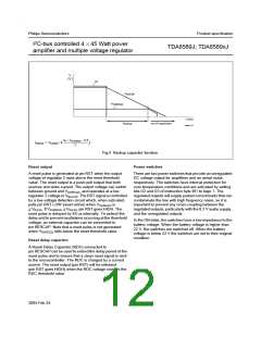
VO REG2
tbackup = Cbackup RL
Example: VP = 14.4 V, VO(REG2) = 5 V, RL = 1 k and
Cbackup = 100 F provides a tbackup of 177 ms.
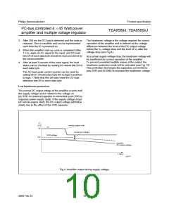
When an overvoltage condition occurs, the voltage on
pin BUCAP is limited to approximately 24 V; see Fig.5.
regulator 2 will switch off and the device will be able to
supply a minimum current for an indefinite amount of time
sufficient for powering the memory of a microcontroller.
Provision is made for an external reserve supply capacitor
to be connected to pin BUCAP which can store enough
energy to allow regulator 2 to supply a microcontroller for
a period long enough for it to prepare for a loss-of-voltage.
Regulator 2
Regulator 2 is intended to supply the microcontroller and
has a low quiescent current. This supply cannot be shut
down in response to overvoltage stress conditions, and is
not I2C-bus controllable to prevent the microcontroller from
being damaged by overvoltage which could occur during a
disturbance of the I2C-bus. This supply will not shut down
during load dump transients or during a high
thermal-protection condition.
Backup capacitor
The backup capacitor is used as a backup supply for the
regulator 2 output when the battery supply voltage (VP)
cannot support the regulator 2 voltage.
2004 Feb 24
11

 NXP [ NXP ]