Philips Semiconductors
Product specication
I2C-bus controlled 4 45 Watt power
amplier and multiple voltage regulator
TDA8589J; TDA8589xJ
FUNCTIONAL DESCRIPTION
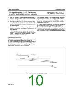
Power-on reset and supply voltage spikes (see Fig.13
and (see Fig.14))
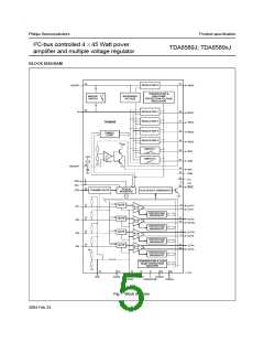
The TDA8589 is a multiple voltage regulator combined
with four independent audio power amplifiers configured in
bridge tied load with diagnostic capability. The output
voltages of all regulators except regulators 2 and 3 can be
controlled via the I2C-bus. However, regulator 3 can be set
to 0 V via the I2C-bus. The output voltage of regulator 2
(microcontroller supply) and the maximum output voltage
of regulator 3 (mechanical digital and microcontroller
supplies) can both be either 5 V or 3.3 V depending on the
type number. The maximum output voltages of both
regulators are fixed to avoid any risk of damaging the
microcontroller that may occur during a disturbance of the
I2C-bus.
If the supply voltage drops too low to guarantee the
integrity of the data in the I2C-bus latches, the power-on
reset cycle will start. All latches will be set to a pre-defined
state, pin DIAG will be pulled LOW to indicate that a
power-on reset has occurred, and bit D7 of data byte 2 is
also set for the same reason. When D0 of instruction
byte 1 is set, the power-on flag resets, pin DIAG is
released and the amplifier will then enter its start-up cycle.
Diagnostic output
Pin DIAG indicates clipping, thermal protection
pre-warning of amplifier and voltage regulator sections,
short-circuit protection, low and high battery voltage.
Pin DIAG is an open-drain output, is active LOW, and must
be connected to an external voltage via an external pull-up
resistor. If a failure occurs, pin DIAG remains LOW during
the failure and no clipping information is available. The
microcontroller can read the failure information via the
I2C-bus.
The amplifier diagnostic functions give information about
output offset, load, or short-circuit. Diagnostic functions
are controlled via the I2C-bus. The TDA8589 is protected
against short-circuit, over-temperature, open ground and
open VP connections. If a short-circuit occurs at the input
or output of a single amplifier, that channel shuts down,
and the other channels continue to operate normally. The
channel that has a short-circuit can be disabled by the
microcontroller via the appropriate enable bit of the
I2C-bus to prevent any noise generated by the fault
condition from being heard.
AMPLIFIERS
Muting
A hard mute and a soft mute can both be performed via the
I2C-bus. A hard mute mutes the amplifier within 0.5 ms.
A soft mute mutes the amplifier within 20 ms and is less
audible. A hard mute is also activated if a voltage of 8 V is
applied to pin STB.
Start-up
At power on, regulator 2 will reach its final voltage when
the backup capacitor voltage exceeds 5.5 V independently
of the voltage on pin STB. When pin STB is LOW, the total
quiescent current is low, and the I2C-bus lines are high
impedance.
Temperature protection
When pin STB is HIGH, the I2C-bus is biased on and then
the TDA8589 performs a power-on reset. When bit D0 of
instruction byte IB1 is set, the amplifier is activated, bit D7
of data byte 2 (power-on reset occurred) is reset, and
pin DIAG is no longer held LOW.
If the average junction temperature rises to a temperature
value that has been set via the I2C-bus, a thermal
protection pre-warning is activated making pin DIAG LOW.
If the temperature continues to rise, all four channels will
be muted to reduce the output power (soft thermal
clipping). The value at which the temperature mute control
activates is fixed; only the temperature at which the
thermal protection pre-warning signal occurs can be
specified by bit D4 in instruction byte 3. If implementing
the temperature mute control does not reduce the average
junction temperature, all the power stages will be switched
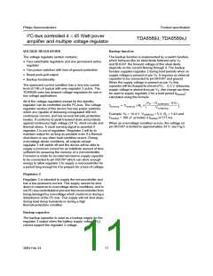
Start-up and shut-down timing (see Fig.12)
A capacitor connected to pin SVR enables smooth start-up
and shut-down, preventing the amplifier from producing
audible clicks at switch-on or switch-off. The start-up and
shut-down times can be extended by increasing the
capacitor value.
off (muted) at the absolute maximum temperature Tj(max)
.
If the amplifier is shut down using pin STB, the amplifier is
muted, the regulators and switches are switched off, and
the capacitor connected to pin SVR discharges. The low
current standby mode is activated 2 seconds after pin STB
goes LOW.
Offset detection
Offset detection can only be performed when there is no
input signal to the amplifiers, for instance when the
external digital signal processor is muted after a start-up.
The output voltage of each channel is measured and
2004 Feb 24
8

 NXP [ NXP ]