Philips Semiconductors
Product specification
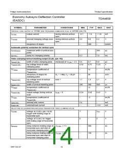
Economy Autosync Deflection Controller
(EASDC)
TDA4858
• Feedback mode (see Fig.12)
B+ control function block
In this application the OTA is used as an error amplifier
with a limited output voltage range. The flip-flop will be
set at the rising edge of the signal at HDRV. A reset will
be generated when the voltage at BSENS taken from
the current sense resistor exceeds the voltage at BOP.
The B+ control function block of the EASDC consists of an
Operational Transconductance Amplifier (OTA), a voltage
comparator, a flip-flop and a discharge circuit. This
configuration allows easy applications for different
B+ control concepts.
If no reset is generated within a line period, the rising
edge of the next HDRV pulse forces the flip-flop to reset.
The flip-flop is set immediately after the voltage at
BSENS has dropped below the threshold voltage
GENERAL DESCRIPTION
The non-inverting input of the OTA is connected internally
to a high precision reference voltage. The inverting input is
connected to BIN (pin 5). An internal clamping circuit limits
the maximum positive output voltage of the OTA.
The output itself is connected to BOP (pin 3) and to the
inverting input of the voltage comparator.
VRESTART(BSENS)
.
• Feed forward mode (see Fig.13)
This application uses an external RC combination at
BSENS to provide a pulse width which is independent
from the horizontal frequency. The capacitor is charged
via an external resistor and discharged by the internal
discharge circuit. For normal operation the discharge
circuit is activated when the flip-flop is reset by the
internal voltage comparator. Now the capacitor will be
discharged with a constant current until the internally
controlled stop level VSTOP(BSENS) is reached. This level
will be maintained until the rising edge of the next HDRV
pulse sets the flip-flop again and disables the discharge
circuit.
The non-inverting input of the voltage comparator can be
accessed via BSENS (pin 4).
B+ drive pulses are generated by an internal flip-flop and
fed to BDRV (pin 6) via an open collector output stage.
This flip-flop will be set at the rising edge of the signal at
HDRV (pin 7). The falling edge of the output signal at
BDRV has a defined delay of td(BDRV) to the rising edge of
the HDRV pulse. When the voltage at BSENS exceeds the
voltage at BOP, the voltage comparator output resets the
flip-flop, and therefore the open collector stage at BDRV is
floating again.
If no reset is generated within a line period, the rising
edge of the next HDRV pulse automatically starts the
discharge sequence and resets the flip-flop (Fig.13).
When the voltage at BSENS reaches the threshold
voltage VRESTART(BSENS), the discharge circuit will be
disabled automatically and the flip-flop will be set
immediately. This behaviour allows a definition of the
maximum duty cycle of the B+ control drive pulse by the
relationship of charge current to discharge current.
An internal discharge circuit allows a well defined
discharge of capacitors at BSENS. BDRV is active at a low
level output voltage (see Figs 12 and 13), thus it requires
an external inverting driver stage.
The B+ function block can be used for B+ deflection
modulators in either of two modes:
1997 Oct 27
10

 NXP [ NXP ]