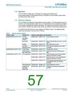
LPC546xx
NXP Semiconductors
32-bit ARM Cortex-M4 microcontroller
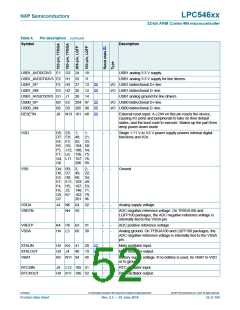
[1] PU = input mode, pull-up enabled (pull-up resistor pulls up pin to VDD). Z = high impedance; pull-up or pull-down disabled, AI = analog
input, I = input, O = output, F = floating. Reset state reflects the pin state at reset without boot code operation. For pin states in the
different power modes, see Section 6.2.2 “Pin states in different power modes”. For termination on unused pins, see Section 6.2.1
“Termination of unused pins”.
[2] 5 V tolerant pad with programmable glitch filter (5 V tolerant if VDD present; if VDD not present, do not exceed 3.6 V); provides digital I/O
functions with TTL levels and hysteresis; normal drive strength. See Figure 44. Pulse width of spikes or glitches suppressed by input
filter is from 3 ns to 16 ns (simulated value).
[3] True open-drain pin. I2C-bus pins compliant with the I2C-bus specification for I2C standard mode, I2C Fast-mode, and I2C Fast-mode
Plus. The pin requires an external pull-up to provide output functionality. When power is switched off, this pin is floating and does not
disturb the I2C lines. Open-drain configuration applies to all functions on this pin.
[4] 5 V tolerant pin providing standard digital I/O functions with configurable modes, configurable hysteresis, and analog input. When
configured as an analog input, the digital section of the pin is disabled, and the pin is not 5 V tolerant.
[5] Reset pad.5 V tolerant pad with glitch filter with hysteresis. Pulse width of spikes or glitches suppressed by input filter is from 3 ns to
20 ns (simulated value)
[6] 5 V tolerant transparent analog pad.
[7] The oscillator input pin (XTALIN) cannot be driven by an external clock. Must connect a crystal between XTALIN and XTALOUT.
[8] VBUS must be connected to supply voltage when using the USB peripheral.
6.2.1 Termination of unused pins
Table 5 shows how to terminate pins that are not used in the application. In many cases,
unused pins should be connected externally or configured correctly by software to
minimize the overall power consumption of the part.
Unused pins with GPIO function should be configured as outputs set to LOW with their
internal pull-up disabled. To configure a GPIO pin as output and drive it LOW, select the
GPIO function in the IOCON register, select output in the GPIO DIR register, and write a 0
to the GPIO PORT register for that pin. Disable the pull-up in the pin’s IOCON register.
In addition, it is recommended to configure all GPIO pins that are not bonded out on
smaller packages as outputs driven LOW with their internal pull-up disabled.
Table 5.
Pin
Termination of unused pins
Default Recommended termination of unused pins
state[1]
RESET
I; PU
The RESET pin can be left unconnected if the application does not use it.
all PIOn_m (not open-drain) I; PU
Can be left unconnected if driven LOW and configured as GPIO output with pull-up
disabled by software.
PIOn_m (I2C open-drain)
RTCXIN
IA
-
Can be left unconnected if driven LOW and configured as GPIO output by software.
Connect to ground. When grounded, the RTC oscillator is disabled.
RTCXOUT
XTALIN
-
Can be left unconnected.
-
Connect to ground. When grounded, the RTC oscillator is disabled.
XTALOUT
VREFP
-
Can be left unconnected.
Tie to VDD.
-
VREFN
-
Tie to VSS.
VDDA
-
Tie to VDD.
VSSA
-
Tie to VSS.
VBAT
-
Tie to VDD.
USBn_DP
F
Can be left unconnected. If USB interface is not used, pin can be left unconnected
except in deep power-down mode where it must be externally pulled low. When the
USB PHY is disabled, the pins are floating.
LPC546xx
All information provided in this document is subject to legal disclaimers.
© NXP Semiconductors N.V. 2018. All rights reserved.
Product data sheet
Rev. 2.5 — 20 June 2018
53 of 169

 NXP [ NXP ]