Nano100(A)
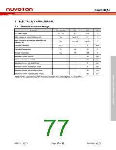
7
ELECTRICAL CHARACTERISTIC
7.1 Absolute Maximum Ratings
SYMBOL
PARAMETER
MIN
-0.3
MAX
+3.6
5.5
UNIT
V
DC Power Supply
VDD
SS
Input Voltage on five-volt tolerance pin
VIN
VIN
VSS -0.3
V
Input Voltage on any other pin without five-volt
tolerance pin
VSS -0.3
VDD +0.3
V
Oscillator Frequency
1/tCLCL
TA
4
24
+85
+150
150
150
25
MHz
C
Operating Temperature
-40
Storage Temperature
TST
-55
C
Maximum Current into VDD
-
-
-
-
-
-
mA
mA
mA
mA
mA
mA
Maximum Current out of VSS
Maximum Current sunk by a I/O pin
Maximum Current sourced by a I/O pin
Maximum Current sunk by total I/O pins
Maximum Current sourced by total I/O pins
25
100
100
Note: GPIO supports input 5V tolerance except ADC shared pins, PC.6 and PC.7.
Mar 31, 2015
Page 77 of 95
Revision V1.00

 NUVOTON [ NUVOTON ]