®
Numonyx™ StrataFlash Embedded Memory (J3-65nm)
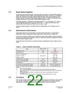
9.0
Erase Operation
Flash erasing is performed on a block basis. An entire block is erased each time an
erase command sequence is issued, and only one block is erased at a time. When a
block is erased, all bits within that block read as logical ones. The following sections
describe block erase operations in detail.
9.1
Block Erase
Erasing a block changes ‘zeros’ to ‘ones’. To change ones to zeros, a program operation
must be performed (see Section 8.0, “Program operation”). Erasing is performed on a
block basis - an entire block is erased each time an erase command sequence is issued.
Once a block is fully erased, all addressable locations within that block read as logical
ones (FFFFh). Only one block-erase operation can occur at a time, and is not permitted
during a program suspend (see Figure 21, “Block Erase Flowchart” on page 61).
Note:
A block-erase operation requires the addressed block to be unlocked, and a valid
voltage applied to VPEN throughout the block-erase operation. Otherwise, the
operation will abort, setting the appropriate Status Register error bit(s).
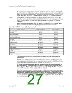
The Erase Confirm command latches the address of the block to be erased. The
addressed block is preconditioned (programmed to all zeros), erased, and then verified.
The read mode of the device is automatically changed to Read Status Register mode,
and remains in effect until another read-mode command is issued.
During a block-erase operation, STS and the Status Register indicates a busy status
(SR.7 = 0). Upon completion, STS and the Status Register indicates a ready status
(SR.7 = 1). The Status Register should be checked for any errors, then cleared. If any
errors did occur, subsequent erase commands to the device are ignored unless the
Status Register is cleared.
The only valid commands during a block erase operation are Read Status and Erase
Suspend. After the block-erase operation has completed, any valid command can be
issued.
Note:
Issuing the Read Array command to the device while it is actively erasing causes
subsequent reads from the device to output invalid data. Valid array data is output only
after the block-erase operation has finished.
Standby power levels are not realized until the block-erase operation has finished. Also,
asserting RP# aborts the block-erase operation, and array contents at the addressed
location are indeterminate. The addressed block should be erased before programming
within the block is attempted.
9.2
Suspend/Resume
An erase or programming operation can be suspended to perform other operations, and
then subsequently resumed. Table 8 shows the Suspend and Resume command bus-
cycles (see Figure 18, “Program/Erase Suspend/Resume Flowchart” on page 57).
Note:
All erase and programming operations require the addressed block to remain unlocked
with a valid voltage applied to VPEN throughout the suspend operation. Otherwise, the
block-erase or programming operation will abort, setting the appropriate Status
Register error bit(s). Also, asserting RP# aborts suspended block-erase and
programming operations, rendering array contents at the addressed location(s)
indeterminate.
Datasheet
26
December 2008
319942-02

 NUMONYX [ NUMONYX B.V ]