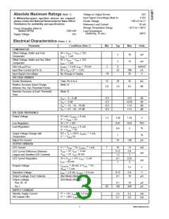
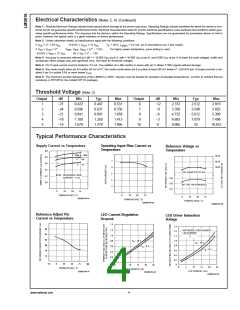
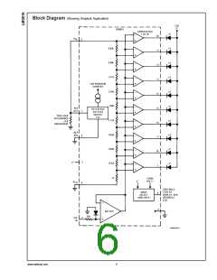
Functional Description
LM3915 Output Circuit
The simplified LM3915 block diagram is included to give the
general idea of the circuit’s operation. A high input imped-
ance buffer operates with signals from ground to 12V, and is
protected against reverse and overvoltage signals. The sig-
nal is then applied to a series of 10 comparators; each of
which is biased to a different comparison level by the resistor
string.
In the example illustrated, the resistor string is connected to
the internal 1.25V reference voltage. In this case, for each
3 dB that the input signal increases, a comparator will switch
on another indicating LED. This resistor divider can be con-
nected between any 2 voltages, providing that they are at
least 1.5V below V+ and no lower than V−.
DS005104-6
Outputs may be run in saturation with no adverse effects,
making it possible to directly drive logic. The effective satura-
tion resistance of the output transistors, equal to RE plus the
transistors’ collector resistance, is about 50Ω. It’s also pos-
sible to drive LEDs from rectified AC with no filtering. To
avoid oscillations, the LED supply should be bypassed with a
2.2 µF tantalum or 10 µF aluminum electrolytic capacitor.
INTERNAL VOLTAGE REFERENCE
The reference is designed to be adjustable and develops a
nominal 1.25V between the REF OUT (pin 7) and REF ADJ
(pin 8) terminals. The reference voltage is impressed across
program resistor R1 and, since the voltage is constant, a
constant current I1 then flows through the output set resistor
R2 giving an output voltage of:
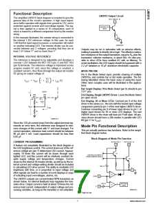
MODE PIN USE
Pin 9, the Mode Select input, permits chaining of multiple
LM3915s, and controls bar or dot mode operation. The fol-
lowing tabulation shows the basic ways of using this input.
Other more complex uses will be illustrated in the applica-
tions.
Bar Graph Display: Wire Mode Select (pin 9) directly to pin
3 (V+ pin).
Dot Display, Single LM3915 Driver: Leave the Mode Select
pin open circuit.
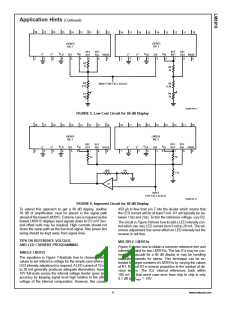
Dot Display, 20 or More LEDs: Connect pin 9 of the first
driver in the series (i.e., the one with the lowest input voltage
comparison points) to pin 1 of the next higher LM3915 driver.
Continue connecting pin 9 of lower input drivers to pin 1 of
higher input drivers for 30 or more LED displays. The last
LM3915 driver in the chain will have pin 9 left open. All pre-
vious drivers should have a 20k resistor in parallel with LED
DS005104-5
#
9 (pin 11 to VLED).
Since the 120 µA current (max) from the adjust terminal rep-
resents an error term, the reference was designed to mini-
mize changes of this current with V+ and load changes. For
correct operation, reference load current should be between
80 µA and 5 mA. Load capacitance should be less than
0.05 µF.
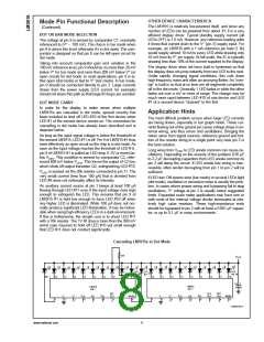
Mode Pin Functional Description
This pin actually performs two functions. Refer to the simpli-
fied block diagram below.
Block Diagram of Mode Pin Function
CURRENT PROGRAMMING
A feature not completely illustrated by the block diagram is
the LED brightness control. The current drawn out of the ref-
erence voltage pin (pin 7) determines LED current. Approxi-
mately 10 times this current will be drawn through each
lighted LED, and this current will be relatively constant de-
spite supply voltage and temperature changes. Current
drawn by the internal 10-resistor divider, as well as by the ex-
ternal current and voltage-setting divider should be included
in calculating LED drive current. The ability to modulate LED
brightness with time, or in proportion to input voltage and
other signals can lead to a number of novel displays or ways
of indicating input overvoltages, alarms, etc.
The LM3915 outputs are current-limited NPN transistors as
shown below. An internal feedback loop regulates the tran-
sistor drive. Output current is held at about 10 times the ref-
erence load current, independent of output voltage and pro-
cessing variables, as long as the transistor is not saturated.
DS005104-7
*
High for bar
7
www.national.com

 NSC [ National Semiconductor ]