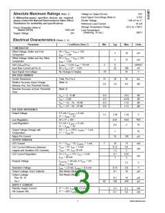
Electrical Characteristics (Notes 2, 4) (Continued)
Note 1: Absolute Maximum Ratings indicate limits beyond which damage to the device may occur. Operating Ratings indicate conditions for which the device is func-
tional, but do not guarantee specific performance limits. Electrical Characteristics state DC and AC electrical specifications under particular test conditions which guar-
antee specific performance limits. This assumes that the device is within the Operating Ratings. Specifications are not guaranteed for parameters where no limit is
given, however, the typical value is a good indication of device performance.
Note 2: Unless otherwise stated, all specifications apply with the following conditions:
+
=
=
25˚C, I
L(REF)
3 V
3 V
≤ V ≤ 20 V
−0.015V ≤ V
≤ 12 V
T
0.2 mA, pin 9 connected to pin 3 (bar mode).
DC
DC
DC
RLO
RLO
DC
A
+
+
≤ V
≤ V
V
, V , V
≤ (V − 1.5V)
For higher power dissipations, pulse testing is used.
LED
REF
RHI
+
−0.015V ≤ V
≤ 12 V
0V ≤ V ≤ V − 1.5V
RHI
DC
IN
=
Note 3: Accuracy is measured referred to 0 dB + 10.000 V at pin 5, with + 10.000 V at pin 6, and 0.000 V at pin 4. At lower full scale voltages, buffer and
DC
DC
DC
comparator offset voltage may add significant error. See table for threshold voltages.
±
±
Note 4: Pin 5 input current must be limited to 3 mA. The addition of a 39k resistor in series with pin 5 allows 100V signals without damage.
+
+
Note 5: Bar mode results when pin 9 is within 20 mV of V . Dot mode results when pin 9 is pulled at least 200 mV below V . LED #10 (pin 10 output current) is dis-
abled if pin 9 is pulled 0.9V or more below V
.
LED
Note 6: The maximum junction temperature of the LM3915 is 100˚C. Devices must be derated for operation at elevated temperatures. Junction to ambient thermal
resistance is 55˚C/W for the molded DIP (N package).
Threshold Voltage (Note 3)
Output
dB
−27
−24
−21
−18
−15
Min
Typ
Max
Output
dB
−12
−9
−6
−3
0
Min
Typ
2.512
3.548
5.012
7.079
10
Max
2.819
3.825
5.309
7.498
10.015
1
2
3
4
5
0.422
0.596
0.841
1.189
1.679
0.447
0.631
0.891
1.259
1.778
0.531
0.750
1.059
1.413
1.995
6
7
2.372
3.350
4.732
6.683
9.985
8
9
10
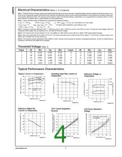
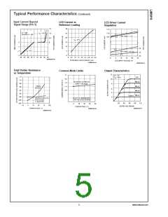
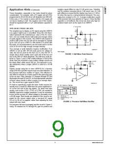
Typical Performance Characteristics
Supply Current vs Temperature
Operating Input Bias Current vs
Temperature
Reference Voltage vs
Temperature
DS005104-34
DS005104-35
DS005104-36
Reference Adjust Pin
Current vs Temperature
LED Current-Regulation
Dropout
LED Driver Saturation
Voltage
DS005104-37
DS005104-38
DS005104-39
www.national.com
4

 NSC [ National Semiconductor ]