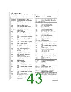
13.0 Memory Map
All RAM, ports and registers (except A and PC) are mapped into data memory address space.
Address
Contents
Address
Contents
S/ADD REG
xxC9
S/ADD REG
0000 to 006F
0070 to 007F
MIWU Enable Register (Reg:WKEN)
MIWU Pending Register (Reg:WKPND)
On-Chip RAM bytes (112 bytes)
xxCA
Unused RAM Address Space (Reads As
All Ones)
xxCB to xxCF Reserved
xxD0
xxD1
xxD2
xxD3
xxD4
xxD5
xxD6
xxD7
Port L Data Register
xx80 to xx93
Unused RAM Address Space (Reads
Undefined Data)
Port L Configuration Register
Port L Input Pins (Read Only)
Reserved for Port L
xx94
Port F data register, PORTFD
xx95
Port F configuration register, PORTFC
Port F input pins (read only), PORTFP
xx96
Port G Data Register
xx97 to xxAF
Unused address space (Reads
Undefined Data)
Port G Configuration Register
Port G Input Pins (Read Only)
xxB0
xxB1
xxB2
Timer T3 Lower Byte
Timer T3 Upper Byte
Port I Input Pins (Read Only) (Actually
reads Port F input pins)
Timer T3 Autoload Register T3RA Lower
Byte
xxD8
xxD9
xxDA
xxDB
xxDC
Port C Data Register
Port C Configuration Register
Port C Input Pins (Read Only)
Reserved for Port C
Port D
xxB3
xxB4
xxB5
Timer T3 Autoload Register T3RA Upper
Byte
Timer T3 Autoload Register T3RB Lower
Byte
xxDD to xxDF Reserved for Port D
Timer T3 Autoload Register T3RB Upper
Byte
xxE0 to xxE5
xxE6
Reserved for EE Control Registers
Timer T1 Autoload Register T1RB Lower
Byte
xxB6
xxB7
Timer T3 Control Register
Comparator Select Register
(Reg:CMPSL)
xxE7
Timer T1 Autoload Register T1RB Upper
Byte
xxB8
xxB9
xxBA
UART Transmit Buffer (Reg:TBUF)
UART Receive Buffer (Reg:RBUF)
xxE8
xxE9
xxEA
xxEB
xxEC
ICNTRL Register
MICROWIRE/PLUS Shift Register
Timer T1 Lower Byte
UART Control and Status Register
(Reg:ENU)
Timer T1 Upper Byte
xxBB
xxBC
UART Receive Control and Status
Register (Reg:ENUR)
Timer T1 Autoload Register T1RA Lower
Byte
UART Interrupt and Clock Source
Register (Reg:ENUI)
xxED
Timer T1 Autoload Register T1RA Upper
Byte
xxBD
xxBE
UART Baud Register (Reg:BAUD)
xxEE
CNTRL Control Register
PSW Register
UART Prescale Select Register
(Reg:PSR)
xxEF
xxF0 to FB
xxFC
On-Chip RAM Mapped as Registers
X Register
xxBF
xxC0
xxC1
xxC2
Reserved for UART
Timer T2 Lower Byte
Timer T2 Upper Byte
xxFD
SP Register
xxFE
B Register
Timer T2 Autoload Register T2RA Lower
Byte
xxFF
S Register
xxC3
xxC4
xxC5
Timer T2 Autoload Register T2RA Upper
Byte
0100–017F
0200–027F
On-Chip 128 RAM Bytes
On-Chip 128 RAM Bytes (Reads as
undefined data on COP8FGE)
Timer T2 Autoload Register T2RB Lower
Byte
0300–037F
On-Chip 128 RAM Bytes (Reads as
undefined data on COP8FGE)
Timer T2 Autoload Register T2RB Upper
Byte
Note: Reading memory locations 0070H–007FH (Segment 0) will return all
ones. Reading unused memory locations 0080H–0093H (Segment 0)
will return undefined data. Reading memory locations from other Seg-
ments (i.e., Segment 4, Segment 5, … etc.) will return undefined data.
xxC6
xxC7
Timer T2 Control Register
WATCHDOG Service Register
(Reg:WDSVR)
xxC8
MIWU Edge Select Register
(Reg:WKEDG)
43
www.national.com

 NSC [ National Semiconductor ]