Functional Description (Continued)
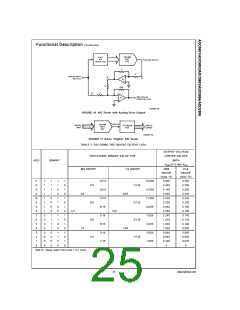
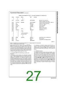
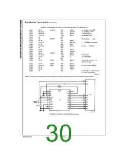
SAMPLE PROGRAM FOR Figure 12 ADC0801–INS8080A CPU INTERFACE
DS005671-99
Note 18: The stack pointer must be dimensioned because a RST 7 instruction pushes the PC onto the stack.
Note 19: All address used were arbitrarily chosen.
The standard control bus signals of the 8080 CS, RD and
WR) can be directly wired to the digital control inputs of the
A/D and the bus timing requirements are met to allow both
starting the converter and outputting the data onto the data
bus. A bus driver should be used for larger microprocessor
systems where the data bus leaves the PC board and/or
must drive capacitive loads larger than 100 pF.
It is important to note that in systems where the A/D con-
verter is 1-of-8 or less I/O mapped devices, no address de-
coding circuitry is necessary. Each of the 8 address bits (A0
to A7) can be directly used as CS inputs — one for each I/O
device.
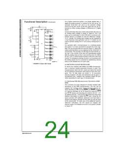
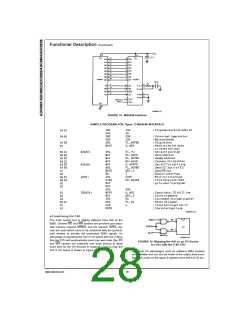
4.1.2 INS8048 Interface
The INS8048 interface technique with the ADC0801 series
(see Figure 13) is simpler than the 8080A CPU interface.
There are 24 I/O lines and three test input lines in the 8048.
With these extra I/O lines available, one of the I/O lines (bit
0 of port 1) is used as the chip select signal to the A/D, thus
eliminating the use of an external address decoder. Bus con-
trol signals RD, WR and INT of the 8048 are tied directly to
the A/D. The 16 converted data words are stored at on-chip
RAM locations from 20 to 2F (Hex). The RD and WR signals
are generated by reading from and writing into a dummy ad-
dress, respectively. A sample interface program is shown
below.
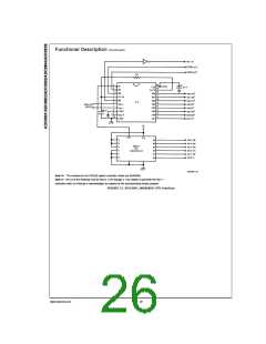
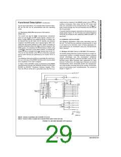
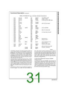
4.1.1 Sample 8080A CPU Interfacing Circuitry and
Program
The following sample program and associated hardware
shown in Figure 12 may be used to input data from the con-
verter to the INS8080A CPU chip set (comprised of the
INS8080A microprocessor, the INS8228 system controller
and the INS8224 clock generator). For simplicity, the A/D is
controlled as an I/O device, specifically an 8-bit bi-directional
port located at an arbitrarily chosen port address, E0. The
TRI-STATE output capability of the A/D eliminates the need
for a peripheral interface device, however address decoding
is still required to generate the appropriate CS for the con-
verter.
27
www.national.com

 NSC [ National Semiconductor ]