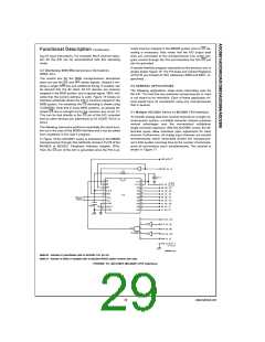
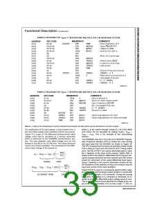
ready memory mapped in the M6800 system and no CS de-
coding is necessary. Also notice that the A/D output data
lines are connected to the microprocessor bus under pro-
gram control through the PIA and therefore the A/D RD pin
can be grounded.
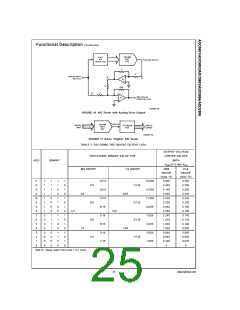
Functional Description (Continued)
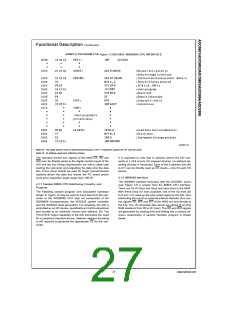
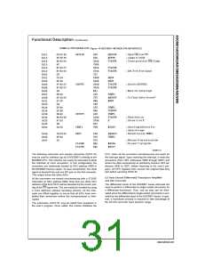
ing I/O input instructions. For example, MUX channel selec-
tion for the A/D can be accomplished with this operating
mode.
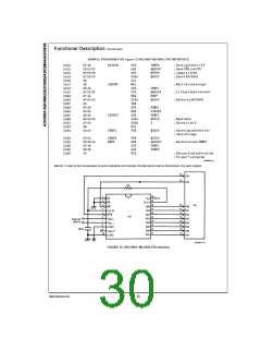
A sample interface program equivalent to the previous one is
shown below Figure 16. The PIA Data and Control Registers
of Port B are located at HEX addresses 8006 and 8007, re-
spectively.
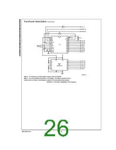
4.3 Interfacing 6800 Microprocessor Derivatives
(6502, etc.)
The control bus for the 6800 microprocessor derivatives
does not use the RD and WR strobe signals. Instead it em-
ploys a single R/W line and additional timing, if needed, can
be derived fom the φ2 clock. All I/O devices are memory
mapped in the 6800 system, and a special signal, VMA, indi-
cates that the current address is valid. Figure 15 shows an
interface schematic where the A/D is memory mapped in the
5.0 GENERAL APPLICATIONS
The following applications show some interesting uses for
the A/D. The fact that one particular microprocessor is used
is not meant to be restrictive. Each of these application cir-
cuits would have its counterpart using any microprocessor
that is desired.
6800 system. For simplicity, the CS decoding is shown using
1
⁄2 DM8092. Note that in many 6800 systems, an already de-
coded 4/5 line is brought out to the common bus at pin 21.
This can be tied directly to the CS pin of the A/D, provided
that no other devices are addressed at HX ADDR: 4XXX or
5XXX.
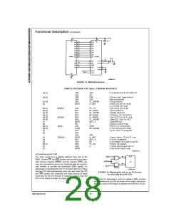
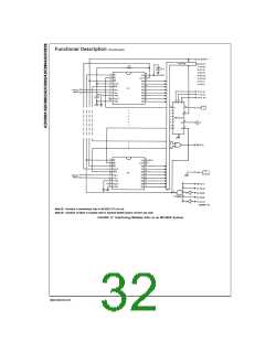
5.1 Multiple ADC0801 Series to MC6800 CPU Interface
To transfer analog data from several channels to a single mi-
croprocessor system, a multiple converter scheme presents
several advantages over the conventional multiplexer
single-converter approach. With the ADC0801 series, the dif-
ferential inputs allow individual span adjustment for each
channel. Furthermore, all analog input channels are sensed
simultaneously, which essentially divides the microproces-
sor’s total system servicing time by the number of channels,
since all conversions occur simultaneously. This scheme is
shown in Figure 17.
The following subroutine performs essentially the same func-
tion as in the case of the 8080A interface and it can be called
from anywhere in the user’s program.
In Figure 16 the ADC0801 series is interfaced to the M6800
microprocessor through (the arbitrarily chosen) Port B of the
MC6820 or MC6821 Peripheral Interface Adapter, (PIA).
Here the CS pin of the A/D is grounded since the PIA is al-
DS005671-24
Note 20: Numbers in parentheses refer to MC6800 CPU pin out.
Note 21: Number or letters in brackets refer to standard M6800 system common bus code.
FIGURE 15. ADC0801-MC6800 CPU Interface
29
www.national.com

 NSC [ National Semiconductor ]