For a higher speed test system, or to obtain plotted data, a
digital-to-analog converter is needed for the test set-up. An
accurate 10-bit DAC can serve as the precision voltage
source for the A/D. Errors of the A/D under test can be ex-
pressed as either analog voltages or differences in 2 digital
words.
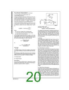
Functional Description (Continued)
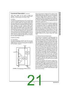
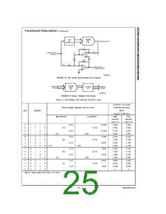
A basic A/D tester that uses a DAC and provides the error as
an analog output voltage is shown in Figure 8. The 2 op
amps can be eliminated if a lab DVM with a numerical sub-
traction feature is available to read the difference voltage,
“A–C”, directly. The analog input voltage can be supplied by
a low frequency ramp generator and an X-Y plotter can be
used to provide analog error (Y axis) versus analog input (X
axis).
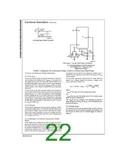
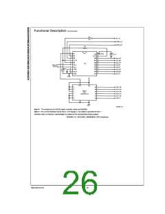
For operation with a microprocessor or a computer-based
test system, it is more convenient to present the errors digi-
tally. This can be done with the circuit of Figure 11, where the
output code transitions can be detected as the 10-bit DAC is
incremented. This provides 1
⁄ LSB steps for the 8-bit A/D un-
4
der test. If the results of this test are automatically plotted
with the analog input on the X axis and the error (in LSB’s)
as the Y axis, a useful transfer function of the A/D under test
results. For acceptance testing, the plot is not necessary and
the testing speed can be increased by establishing internal
limits on the allowed error for each code.
DS005671-18
FIGURE 9. Basic A/D Tester
4.0 MICROPROCESSOR INTERFACING
To dicuss the interface with 8080A and 6800 microproces-
sors, a common sample subroutine structure is used. The
microprocessor starts the A/D, reads and stores the results
of 16 successive conversions, then returns to the user’s pro-
gram. The 16 data bytes are stored in 16 successive
memory locations. All Data and Addresses will be given in
hexadecimal form. Software and hardware details are pro-
vided separately for each type of microprocessor.
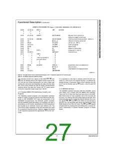
4.1 Interfacing 8080 Microprocessor Derivatives (8048,
8085)
This converter has been designed to directly interface with
derivatives of the 8080 microprocessor. The A/D can be
mapped into memory space (using standard memory ad-
dress decoding for CS and the MEMR and MEMW strobes)
or it can be controlled as an I/O device by using the I/O R
→
and I/O W strobes and decoding the address bits A0
A7
→
(or address bits A8 A15 as they will contain the same 8-bit
address information) to obtain the CS input. Using the I/O
space provides 256 additional addresses and may allow a
simpler 8-bit address decoder but the data can only be input
to the accumulator. To make use of the additional memory
reference instructions, the A/D should be mapped into
memory space. An example of an A/D in I/O space is shown
in Figure 12.
www.national.com
24

 NSC [ National Semiconductor ]