PSMN3R5-80PS
Nexperia
N-channel 80 V, 3.5 mΩ standard level MOSFET in TO-220
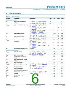
6. Characteristics
Table 6.
Symbol
Characteristics
Parameter
Conditions
Min
Typ
Max
Unit
Static characteristics
V(BR)DSS drain-source breakdown
voltage
ID = 250 µA; VGS = 0 V; Tj = -55 °C
ID = 250 µA; VGS = 0 V; Tj = 25 °C
73
80
1
-
-
-
-
-
-
V
V
V
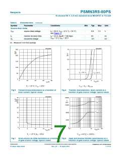
VGS(th)
gate-source threshold voltage ID = 1 mA; VDS = VGS; Tj = 175 °C;
see Figure 10
ID = 1 mA; VDS = VGS; Tj = -55 °C;
see Figure 10
-
-
4.6
4
V
V
ID = 1 mA; VDS = VGS; Tj = 25 °C;
see Figure 10; see Figure 11
2
3
IDSS
drain leakage current
gate leakage current
VDS = 80 V; VGS = 0 V; Tj = 25 °C
VDS = 80 V; VGS = 0 V; Tj = 175 °C
VGS = -20 V; VDS = 0 V; Tj = 25 °C
VGS = 20 V; VDS = 0 V; Tj = 25 °C
-
-
-
-
-
0.02
10
µA
µA
nA
nA
mΩ
-
500
100
100
8.4
IGSS
-
-
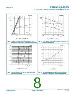
RDSon
drain-source on-state
resistance
VGS = 10 V; ID = 25 A; Tj = 175 °C;
see Figure 12
7.2
VGS = 10 V; ID = 25 A; Tj = 100 °C;
see Figure 12
-
-
-
5
5.8
3.5
-
mΩ
mΩ
Ω
[1]
V
GS = 10 V; ID = 25 A; Tj = 25 °C;
3
see Figure 13
RG
internal gate resistance (AC)
f = 1 MHz
0.9
Dynamic characteristics
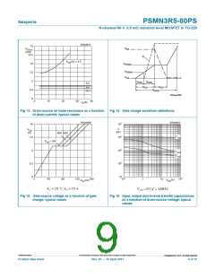
QG(tot)
total gate charge
ID = 0 A; VDS = 0 V; VGS = 10 V
-
-
-
-
135
139
51
-
-
-
-
nC
nC
nC
nC
ID = 75 A; VDS = 40 V; VGS = 10 V;
see Figure 14; see Figure 15
QGS
gate-source charge
QGS(th)
pre-threshold gate-source
charge
30
QGS(th-pl)
post-threshold gate-source
charge
-
21
-
nC
QGD
gate-drain charge
-
-
27
-
-
nC
V
VGS(pl)
gate-source plateau voltage
ID = 25 A; VDS = 40 V; see Figure 14;
see Figure 15
5.8
Ciss
Coss
Crss
td(on)
tr
input capacitance
output capacitance
reverse transfer capacitance
turn-on delay time
rise time
VDS = 40 V; VGS = 0 V; f = 1 MHz;
Tj = 25 °C; see Figure 16
-
-
-
-
-
-
-
9961
847
401
41
-
-
-
-
-
-
-
pF
pF
pF
ns
ns
ns
ns
VDS = 40 V; RL = 0.53 Ω; VGS = 10 V;
RG(ext) = 10 Ω; ID = 75 A
43
td(off)
tf
turn-off delay time
fall time
109
44
PSMN3R5-80PS
All information provided in this document is subject to legal disclaimers.
©
Nexperia B.V. 2017. All rights reserved
Product data sheet
Rev. 03 — 19 April 2011
6 of 15

 NEXPERIA [ Nexperia ]