Nexperia
PMV45EN2
30 V, N-channel Trench MOSFET
8. Limiting values
Table 5. Limiting values
In accordance with the Absolute Maximum Rating System (IEC 60134).
Symbol
VDS
Parameter
Conditions
Min
Max
30
Unit
V
drain-source voltage
gate-source voltage
drain current
Tj = 25 °C
-
VGS
-20
20
V
[1]
[1]
[1]
ID
VGS = 10 V; Tamb = 25 °C; t ≤ 5 s
VGS = 10 V; Tamb = 25 °C
VGS = 10 V; Tamb = 100 °C
Tamb = 25 °C; single pulse; tp ≤ 10 µs
Tamb = 25 °C
-
5.1
A
-
4.1
A
-
2.6
A
IDM
Ptot
peak drain current
-
16
A
[2]
[1]
total power dissipation
-
510
1115
5000
150
150
150
mW
mW
mW
°C
°C
°C
-
Tsp = 25 °C
-
Tj
junction temperature
ambient temperature
storage temperature
-55
-55
-65
Tamb
Tstg
Source-drain diode
IS source current
[1]
Tamb = 25 °C
-
1
A
[1] Device mounted on an FR4 Printed-Circuit Board (PCB), single-sided copper, tin-plated, mounting pad for drain 6 cm2.
[2] Device mounted on an FR4 Printed Circuit Board (PCB), single-sided copper, tin-plated and standard footprint.
017aaa123
017aaa124
120
120
P
I
der
der
(%)
(%)
80
80
40
40
0
- 75
0
- 75
- 25
25
75
125
175
- 25
25
75
125
175
T (°C)
j
T (°C)
j
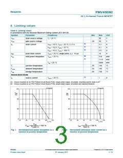
Fig. 1. Normalized total power dissipation as a
function of junction temperature
Fig. 2. Normalized continuous drain current as a
function of junction temperature
©
PMV45EN2
All information provided in this document is subject to legal disclaimers.
Nexperia B.V. 2017. All rights reserved
Product data sheet
10 January 2017
3 / 15

 NEXPERIA [ Nexperia ]