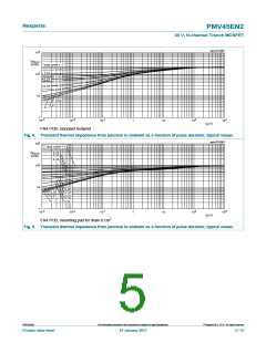
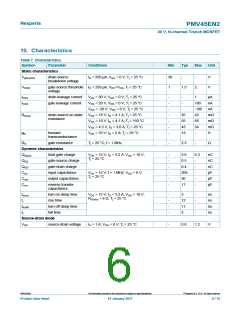
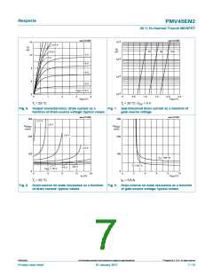
Nexperia
PMV45EN2
30 V, N-channel Trench MOSFET
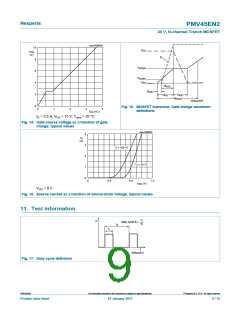
aaa-009050
10
V
DS
V
GS
(V)
I
D
8
6
4
2
0
V
V
GS(pl)
GS(th)
V
GS
Q
GS2
Q
GS1
Q
Q
GD
G(tot)
GS
Q
003aaa508
Fig. 15. MOSFET transistor: Gate charge waveform
definitions
0
1
2
3
4
Q
(nC)
G
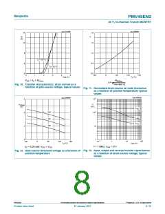
ID = 3.2 A; VDS = 15 V; Tamb = 25 °C
Fig. 14. Gate-source voltage as a function of gate
charge; typical values
aaa-009052
4
I
S
(A)
3
2
1
0
T = 150 °C
j
T = 25 °C
j
0
0.4
0.8
1.2
V
(V)
SD
VGS = 0 V
Fig. 16. Source current as a function of source-drain voltage; typical values
11. Test information
t
t
1
2
P
duty cycle δ =
t
2
t
1
t
006aaa812
Fig. 17. Duty cycle definition
©
PMV45EN2
All information provided in this document is subject to legal disclaimers.
Nexperia B.V. 2017. All rights reserved
Product data sheet
10 January 2017
9 / 15

 NEXPERIA [ Nexperia ]