Nexperia
PMBT3904YS
40 V, 200 mA NPN/NPN general-purpose double transistor
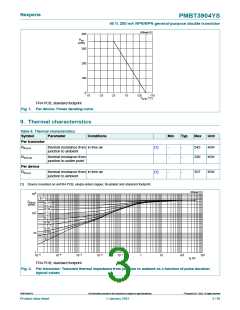
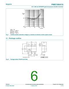
006aab113
400
tot
P
(mW)
300
200
100
0
- 75
- 25
25
75
125
T
175
(°C)
amb
FR4 PCB, standard footprint
Fig. 1. Per device: Power derating curve
9. Thermal characteristics
Table 6. Thermal characteristics
Symbol
Parameter
Conditions
Min
Typ
Max
Unit
Per transistor
Rth(j-a)
thermal resistance from in free air
junction to ambient
[1]
-
-
-
-
543
290
K/W
K/W
Rth(j-sp)
thermal resistance from
junction to solder point
Per device
Rth(j-a)
thermal resistance from in free air
junction to ambient
[1]
-
-
357
K/W
[1] Device mounted on anFR4 PCB, single-sided copper, tin-plated and standard footprint.
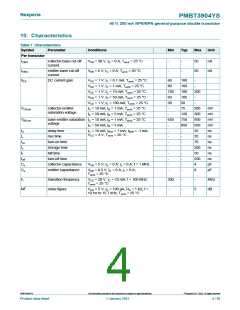
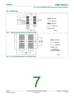
006aab114
3
10
δ = 1
Z
th(j-a)
(K/W)
0.75
0.5
0.33
2
0.2
0.1
10
0.05
0.02
0.01
10
0
1
10
- 5
- 4
- 3
- 2
- 1
2
3
10
10
10
10
1
10
10
10
t
(s)
p
FR4 PCB, standard footprint
Fig. 2. Per transistor: Transient thermal impedance from junction to ambient as a function of pulse duration;
typical values
©
PMBT3904YS
All information provided in this document is subject to legal disclaimers.
Nexperia B.V. 2023. All rights reserved
Product data sheet
1 January 2023
3 / 10

 NEXPERIA [ Nexperia ]