74LVC1G57-Q100
Nexperia
Low-power configurable multiple function gate
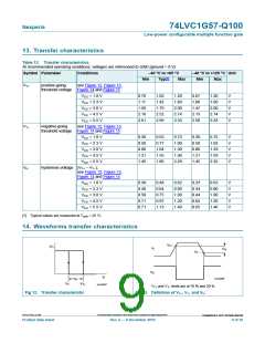
11. Dynamic characteristics
Table 9.
Dynamic characteristics
Voltages are referenced to GND (ground = 0 V); for test circuit, see Figure 11.
Symbol Parameter Conditions 40 C to +85 C
40 C to +125 C Unit
Min
Typ[1]
Max
Min
Max
[2]
tpd
propagation delay A, B, C to Y; see Figure 10
VCC = 1.65 V to 1.95 V
VCC = 2.3 V to 2.7 V
1.0
0.5
0.5
0.5
0.5
-
6.0
3.5
4.2
3.8
3.0
22
14.4
8.3
8.5
6.3
5.1
-
1.0
0.5
0.5
0.5
0.5
-
18
10.4
10.6
7.9
6.4
-
ns
ns
ns
ns
ns
pF
VCC = 2.7 V
VCC = 3.0 V to 3.6 V
VCC = 4.5 V to 5.5 V
[3]
CPD
power dissipation VCC = 3.3 V; VI = GND to VCC
capacitance
[1] Typical values are measured at nominal VCC and at Tamb = 25 C.
[2] tpd is the same as tPLH and tPHL
[3] CPD is used to determine the dynamic power dissipation (PD in W).
PD = CPD VCC2 fi N + (CL VCC2 fo) where:
fi = input frequency in MHz;
fo = output frequency in MHz;
CL = output load capacitance in pF;
VCC = supply voltage in V;
N = number of inputs switching;
(CL VCC2 fo) = sum of outputs.
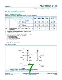
12. Waveforms
9
,
$ꢇꢆ%ꢇꢆ&ꢆLQSXW
*1'
9
9
0
0
W
W
3/+
3+/
3/+
9
2+
9
9
9
0
<ꢆRXWSXW
<ꢆRXWSXW
0
W
9
2/
W
3+/
9
2+
9
0
0
9
2/
ꢀꢀꢁDDEꢂꢆꢄ
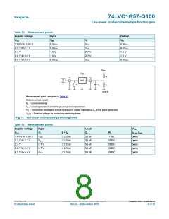
Measurement points are given in Table 10.
VOL and VOH are typical output voltage levels that occur with the output load.
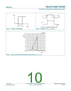
Fig 10. Input A, B and C to output Y propagation delay times
74LVC1G57_Q100
All information provided in this document is subject to legal disclaimers.
©
Nexperia B.V. 2017. All rights reserved
Product data sheet
Rev. 2 — 9 December 2016
7 of 16

 NEXPERIA [ Nexperia ]