74LVC1G57-Q100
Nexperia
Low-power configurable multiple function gate
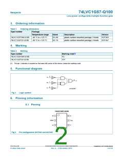
6.2 Pin description
Table 3.
Pin description
Symbol
Pin
1
Description
data input
B
GND
A
2
ground (0 V)
data input
3
Y
4
data output
supply voltage
data input
VCC
C
5
6
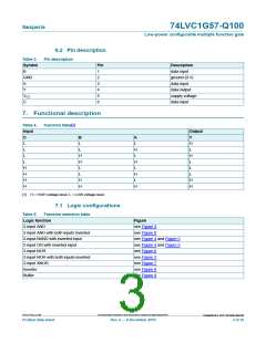
7. Functional description
Table 4.
Function table[1]
Input
Output
C
L
B
L
A
L
Y
H
L
L
L
H
L
L
H
H
L
H
L
L
H
L
H
H
H
H
L
L
H
L
L
H
H
H
H
H
[1] H = HIGH voltage level; L = LOW voltage level.
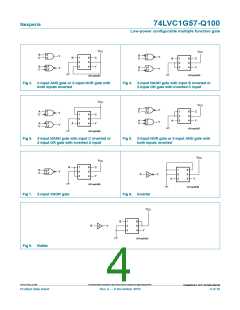
7.1 Logic configurations
Table 5.
Function selection table
Logic function
Figure
2-input AND
see Figure 3
2-input AND with both inputs inverted
2-input NAND with inverted input
2-input OR with inverted input
2-input NOR
see Figure 6
see Figure 4 and Figure 5
see Figure 4 and Figure 5
see Figure 6
2-input NOR with both inputs inverted
2-input XNOR
see Figure 3
see Figure 7
Inverter
see Figure 8
Buffer
see Figure 9
74LVC1G57_Q100
All information provided in this document is subject to legal disclaimers.
©
Nexperia B.V. 2017. All rights reserved
Product data sheet
Rev. 2 — 9 December 2016
3 of 16

 NEXPERIA [ Nexperia ]