µPD75304B,75306B,75308B
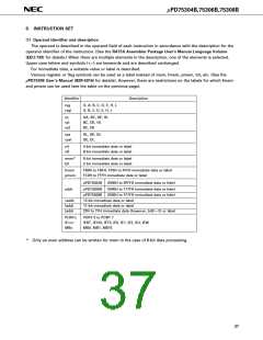
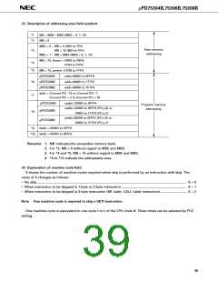
(3) Description of addressing area field symbols
*1
*2
MB = MBE • MBS (MBS = 0, 1, 15)
MB = 0
MBE = 0 : MB = 0 (00H to 7FH)
MB = 15 (80H to FFH)
Data memory
addressing
*3
MBE = 1 : MB = MBS (MBS = 0, 1, 15)
MB = 15, fmem = FB0H to FBFH,
FF0H to FFFH
*4
*5
MB = 15, pmem = FC0H to FFFH
µPD75304B
µPD75306B
µPD75308B
addr=0000H to 0FFFH
addr=0000H to 177FH
addr=0000H to 1F7FH
*6
*7
addr = (Current PC) –15 to (Current PC) –1
(Current PC) + 2 to (Current PC) + 16
µPD75304B
µPD75306B
caddr= 0000H to 0FFFH
Program memory
addressing
caddr= 0000H to 0FFFH (PC12=0) or
1000H to 177FH (PC12=1)
*8
caddr=0000H to 0FFFH (PC12=0) or
1000H to 1F7FH (PC12=1)
µPD75308B
faddr = 0000H to 07FFH
taddr = 0020H to 007FH
*9
*10
Remarks 1. MB indicates the accessible memory bank.
2. For *2, MB = 0 without regard to MBE and MBS.
3. For *4 and *5, MB = 15 without regard to MBE and MBS.
4. *6 to *10 indicate the addressable area.
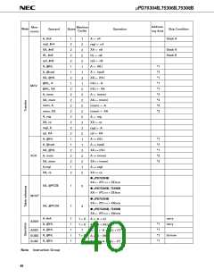
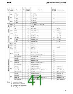
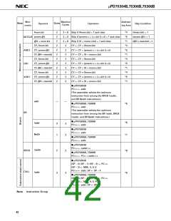
(4) Explanation of machine cycle field
S shows the number of machine cycles required when skip is performed by an instruction with skip. The
value of S changes as follows:
• No skip ....................................................................................................................................................................... S = 0
• When instruction to be skipped is 1-byte or 2-byte instruction ......................................................................... S = 1
• When instruction to be skipped is 3-byte instruction (BR !addr, CALL !addr instruction)............................. S = 2
Note One machine cycle is required to skip a GETI instruction.
One machine cycle is equivalent to one cycle (=tCY) of the CPU clock Φ. Three times can be selected by PCC
setting.
39

 NEC [ NEC ]