µPD703100A-33, 703100A-40, 703101A-33, 703102A-33
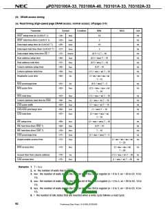
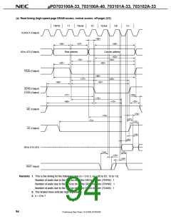
(b) Read timing (high-speed page DRAM access: on-page) (1/2)
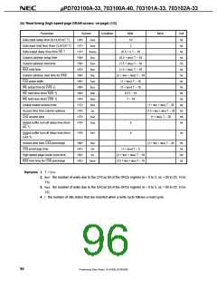
Parameter
Symbol
<26>
Condition
MIN.
10
MAX.
Unit
ns
ns
ns
ns
ns
ns
ns
ns
ns
ns
ns
ns
ns
ns
ns
Data input setup time (to CLKOUT ↑)
Data input hold time (from CLKOUT ↑)
Data output delay time from OE ↑
Column address setup time
Column address hold time
RAS hold time
tSKID
tHKID
tDRDOD
tASC
tCAH
tRSH
tRAL
<27>
<37>
<58>
<59>
<63>
<64>
<65>
<68>
<69>
<70>
<72>
<74>
<75>
<78>
2
(0.5 + i) T – 10
(0.5 + wCP) T – 10
(1.5 + wDA) T – 10
(1.5 + wDA) T – 10
(2 + wCP + wDA) T – 10
(1 + wDA) T – 10
(1 + wCP) T – 10
0.5T – 10
Column address read time for RAS
CAS pulse width
tCAS
tRCS
tRRH
tRCH
tOEA
tAA
WE setup time (to CAS ↓)
WE hold time (from RAS ↑)
WE hold time (from CAS ↑)
Output enable access time
Access time from column address
CAS access time
T – 10
(1 + wCP + wDA) T – 20
(1.5 + wCP + wDA) T – 20
tCAC
tOEZ
(1 + wDA) T – 20
Output buffer turn-off delay time (from
0
0
OE ↑)
Output buffer turn-off delay time (from
<79>
tOFF
ns
CAS ↑)
Access time from CAS precharge
CAS precharge time
<80>
<81>
<82>
<83>
tACP
tCP
(2 + wCP + wDA) T – 20
ns
ns
ns
ns
(1 + wCP) T – 5
High-speed page mode cycle time
RAS hold time for CAS precharge
tPC
(2 + wCP + wDA) T – 10
tRHCP
(2.5 + wCP + wDA) T – 10
Remarks 1. T = tCYK
2. wCP: the number of waits due to the CPCxx bit of the DRCn register (n = 0 to 3, xx = 00 to 03, 10 to
13).
3. wDA: the number of waits due to the DACxx bit of the DRCn register (n = 0 to 3, xx = 00 to 03, 10 to
13).
4. i: the number of idle states that are inserted when a write cycle follows a read cycle.
96
Preliminary Data Sheet U14168EJ2V0DS00

 NEC [ NEC ]