µPD703100A-33, 703100A-40, 703101A-33, 703102A-33
2.3 Pin I/O Circuits and Recommended Connection of Unused Pins
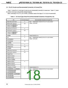
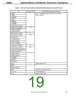
Table 2-1 shows the I/O circuit type of each pin and recommended connection of unused pins. Figure 2-1 shows
the various circuit types using partially abridged diagrams.
When connecting to VDD or VSS via a resistor, a resistance value in the range of 1 to 10 kΩ is recommended.
Table 2-1. I/O Circuit Type of Each Pin and Recommended Connection of Unused Pins (1/2)
Pin
I/O Circuit Type
Recommended Connection of Unused Pins
P00/TO100, P01/TO101
P02/TCLR10, P03/TI10
5
Input: Independently connect to HVDD or VSS via a resistor
Output: Leave open
5-K
P04/INTP100/DMARQ0 to
P07/INTP103/DMARQ3
P10/TO110, P11/TO111
P12/TCLR11, P13/TI11
5
5-K
P14/INTP110/DMAAK0 to
P17/INTP113/DMAAK3
P20/NMI
2
5
Connect directly to VSS
P21
Input: Independently connect to HVDD or VSS via a resistor
Output: Leave open
P22/TXD0/SO0
P23/RXD0/SI0
5-K
P24/SCK0
P25/TXD1/SO1
P26/RXD1/SI1
5
5-K
P27/SCK1
P30/TO130, P31/TO131
P32/TCLR13, P33/TI13
P34/INTP130
5
5-K
P35/INTP131/SO2
P36/INTP132/SI2
P37/INTP133/SCK2
P40/D0 to P47/D7
P50/D8 to P57/D15
P60/A16 to P67/A23
P70/ANI0 to P77/ANI7
P80/CS0/RAS0 to P83/CS3/RAS3
5
9
5
Connect directly to VSS
Input: Independently connect to HVDD or VSS via a resistor
Output: Leave open
P84/CS4/RAS4/IOWR,
P85/CS5/RAS5/IORD
P86/CS6/RAS6, P87/CS7/RAS7
P90/LCAS/LWR
P91/UCAS/UWR
18
Preliminary Data Sheet U14168EJ2V0DS00

 NEC [ NEC ]