µPD703100A-33, 703100A-40, 703101A-33, 703102A-33
(2/4)
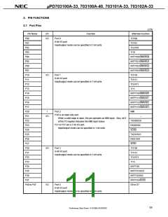
Pin Name
INTP130
I/O
I
Function
Alternate Function
P34
External maskable interrupt request input, also used as external capture
trigger input for timer 13
INTP131
INTP132
INTP133
INTP140
INTP141
INTP142
INTP143
INTP150
INTP151
INTP152
INTP153
SO0
P35/SO2
P36/SI2
P37/SCK2
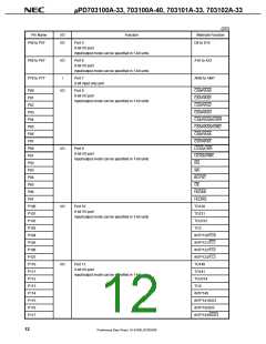
P114
I
I
External maskable interrupt request input, also used as external capture
trigger input for timer 14
P115/SO3
P116/SI3
P117/SCK3
P124
External maskable interrupt request input, also used as external capture
trigger input for timer 15
P125
P126
P127/ADTRG
P22/TXD0
P25/TXD1
P35/INTP131
P115/INTP141
P23/RXD0
P26/RXD1
P36/INTP132
P116/INTP142
P24
O
Serial transmit data output (3-wire) for CSI0 to CSI3
Serial receive data input (3-wire) for CSI0 to CSI3
Serial clock I/O (3-wire) for CSI0 to CSI3
SO1
SO2
SO3
SI0
I
SI1
SI2
SI3
SCK0
I/O
SCK1
P27
SCK2
P37/INTP133
P117/INTP143
P22/SO0
P25/SO1
P23/SI0
SCK3
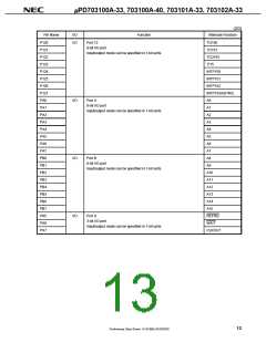
TXD0
O
I
Serial transmit data output for UART0 and UART1
Serial receive data input for UART0 and UART1
16-bit data bus for external memory
TXD1
RXD0
RXD1
P26/SI1
D0 to D7
D8 to D15
A0 to A7
A8 to A15
A16 to A23
LWR
I/O
O
P40 to P47
P50 to P57
PA0 to PA7
PB0 to PB7
P60 to P67
P90/LCAS
P91/UCAS
P92
24-bit address bus for external memory
O
O
O
O
O
Lower byte write-enable signal output for external data bus
Higher byte write-enable signal output for external data bus
Read strobe signal output for external data bus
Write enable signal output for DRAM
UWR
RD
WE
P93
OE
Output enable signal output for DRAM
P95
15
Preliminary Data Sheet U14168EJ2V0DS00

 NEC [ NEC ]