µPD703100A-33, 703100A-40, 703101A-33, 703102A-33
2. PIN FUNCTIONS
2.1 Port Pins
(1/3)
Alternate Function
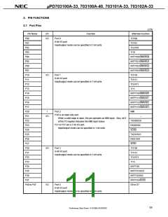
Pin Name
P00
I/O
I/O
Function
Port 0
TO100
8-bit I/O port
P01
TO101
Input/output mode can be specified in 1-bit units
P02
TCLR10
P03
TI10
P04
INTP100/DMARQ0
INTP101/DMARQ1
INTP102/DMARQ2
INTP103/DMARQ3
TO110
P05
P06
P07
P10
I/O
Port 1
8-bit I/O port
P11
TO111
Input/output mode can be specified in 1-bit units
P12
TCLR11
P13
TI11
P14
INTP110/DMAAK0
INTP111/DMAAK1
INTP112/DMAAK2
INTP113/DMAAK3
NMI
P15
P16
P17
P20
I
Port 2
P20 is an input only port.
P21
I/O
–
When a valid edge is input, this pin operates as NMI input. Also, bit 0
of the P2 register indicates the NMI input status.
P21 to P27 are a 7-bit I/O port.
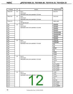
P22
TXD0/SO0
RXD0/SI0
SCK0
P23
Input/output mode can be specified in 1-bit units
P24
P25
TXD1/SO1
RXD1/SI1
SCK1
P26
P27
P30
I/O
Port 3
TO130
8-bit I/O port.
P31
TO131
Input/output mode can be specified in 1-bit units
P32
TCLR13
P33
TI13
P34
INTP130
P35
INTP131/SO2
INTP132/SI2
INTP133/SCK2
D0 to D7
P36
P37
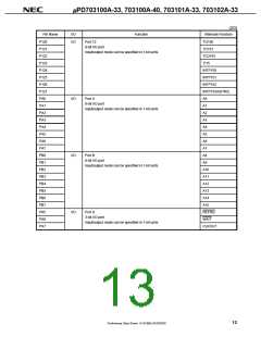
P40 to P47
I/O
Port 4
8-bit I/O port
Input/output mode can be specified in 1-bit units
11
Preliminary Data Sheet U14168EJ2V0DS00

 NEC [ NEC ]