µPD703100A-33, 703100A-40, 703101A-33, 703102A-33
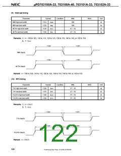
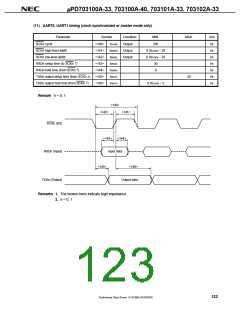
(11) UART0, UART1 timing (clock-synchronized or master mode only)
Parameter
Symbol
<140>
Condition
Output
MIN.
MAX.
Unit
ns
ns
ns
ns
ns
ns
ns
SCKn cycle
tCYSK0
tWSK0H
tWSK0L
tSRXSK
tHSKRX
tDSKTX
tHSKTX
250
SCKn high-level width
<141>
<142>
<143>
<144>
<145>
<146>
Output
0.5tCYSK0 – 20
SCKn low-level width
Output
0.5tCYSK0 – 20
RXDn setup time (to SCKn ↑)
RXDn hold time (from SCKn ↑)
TXDn output delay time (from SCKn ↓)
TXDn output hold time (from SCKn ↑)
30
0
20
0.5tCYSK0 – 5
Remark n = 0, 1
<140>
<142>
<141>
SCKn (I/O)
<143>
<144>
RXDn (Input)
Input data
<145>
<146>
TXDn (Output)
Output data
Remarks 1. The broken lines indicate high impedance.
2. n = 0, 1
123
Preliminary Data Sheet U14168EJ2V0DS00

 NEC [ NEC ]