NTC Proprietary
Level: Property
DDR3(L)-2Gb SDRAM
NT5CB(C)256M8JQ/NT5CB(C)128M16JR
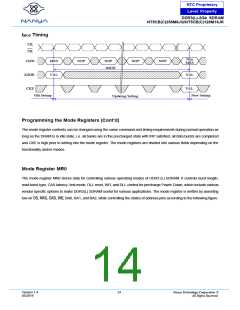
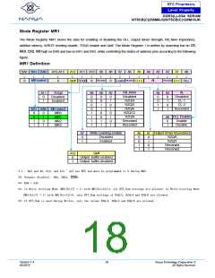
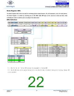
Mode Register MR1
The Mode Register MR1 stores the data for enabling or disabling the DLL, output driver strength, Rtt_Nom impedance,
additive latency, WRITE leveling enable, TDQS enable and Qoff. The Mode Register 1 is written by asserting low on ,
RA, A, WE high on BA0 and low on BA1 and BA2, while controlling the states of address pins according to the following
figure.
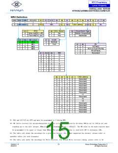
MR1 Definition
BA2 BA1 BA0
A15-A13
A12 A11 A10 A9
A8
↓
0
A7
↓
A6
A5
↓
A4
A3
A2
A1
A0
↓
↓
↓
↓
↓
↓
↓
↓
↓
Rtt_Nom
↓
↓
↓
Rtt_Nom
↓
↓
Rtt_Nom
MR select
AL
0
0
Qoff TDQS
0
Level
D.I.C
D.I.C DLL
Rtt_Nom
Disabled
RZQ/4
AL
Disabled
CL-1
A11
0
1
TDQS
Disabled
Enabled
A9
0
0
A6
0
0
A2
0
1
A4
0
0
A3
0
1
RZQ/2
CL-2
0
1
0
1
0
RZQ/6
Reserved
BA1 BA0 MR select
0
1
1
1
1
RZQ/12
RZQ/8
Reserved
Reserved
0
0
1
1
0
1
0
1
MR0
MR1
MR2
MR3
1
1
1
1
0
0
1
1
0
1
0
1
DLL Enable
Enable
Disable
A0
0
1
Write Leveling enable
Disabled
Output Driver Impedance
RZQ/6
A7
0
A5
0
A1
0
Enabled
RZQ/7
1
0
1
Reserved
1
0
Reserved
1
1
Qoff
A12
Output buffer enabled
Output buffer disabled
0
1
* 1 : BA2 and A8, A10, and A13 ~ A15 are RFU and must be programmed to 0 during MRS.
*2: Outputs disabled - DQs, DQSs, s.
*3: RZQ = 240
*4: In Write leveling Mode (MR1[bit7] = 1) with MR1[bit12]=1, all RTT_Nom settings are allowed; in Write Leveling Mode
(MR1[bit7] = 1) with MR1[bit12]=0, only RTT_Nom settings of RZQ/2, RZQ/4 and RZQ/6 are allowed.
*5: If RTT_Nom is used during Writes, only the values RZQ/2, RZQ/4 and RZQ/6 are allowed.
Version 1.4
05/2019
18
Nanya Technology Cooperation ©
All Rights Reserved.

 NANYA [ Nanya Technology Corporation. ]