NTC Proprietary
Level: Property
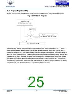
DDR3(L)-2Gb SDRAM
NT5CB(C)256M8JQ/NT5CB(C)128M16JR
Write leveling
For better signal integrity, DDR3(L) memory module adopted fly by topology for the commands, addresses, control signals,
and clocks. The fly by topology has benefits from reducing number of stubs and their length but in other aspect, causes
flight time skew between clock and strobe at every DRAM on DIMM. It makes difficult for the Controller to maintain tDQSS,
tDSS, and tDSH specification. Therefore, the controller should support ‘write leveling’ in DDR3(L) SDRAM to compensate
for skew.
Output Disable
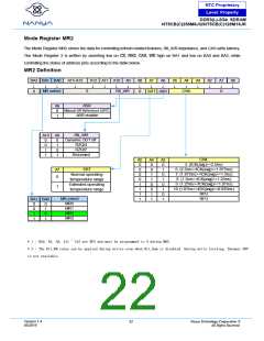
The DDR3(L) SDRAM outputs maybe enable/disabled by MR1 (bit12) as shown in MR1 definition. When this feature is
enabled (A12=1) all output pins (DQs, DQS, , etc.) are disconnected from the device removing any loading of the output
drivers. This feature may be useful when measuring modules power for example. For normal operation A12 should be set
to ‘0’.
TDQS, T
TDQS (Termination Data Strobe) is a feature of x8 DDR3(L) SDRAM that provides additional termination resistance outputs
that may be useful in some system configurations.
When enabled via the mode register, the same termination resistance function is applied to be TDQS/T pins that are
applied to the DQS/ pins.
In contrast to the RDQS function of DDR2 SDRAM, TDQS provides the termination resistance function only. The data strobe
function of RDQS is not provided by TDQS.
The TDQS and DM functions share the same pin. When the TDQS function is enabled via the mode register, the DM function
is not supported. When the TDQS function is disabled, the DM function is provided and the T pin is not used.
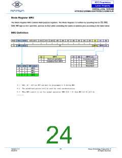
The TDQS function is available in x8 DDR3(L) SDRAM only and must be disabled via the mode register A11=0 in MR1 for
x16 configurations.
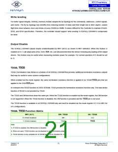
TDQS, T Function Matrix
MR1 (A11)
DM / TDQS
DM
NU / TDQS
Hi-Z
0 (TDQS Disabled)
1 (TDQS Enabled)
TDQS
T
Note:
1. If TDQS is enabled, the DM function is disabled.
2. When not used, TDQS function can be disabled to save termination power.
3. TDQS function is only available for x8 DRAM and must be disabled for x16.
Version 1.4
05/2019
21
Nanya Technology Cooperation ©
All Rights Reserved.

 NANYA [ Nanya Technology Corporation. ]